The article describes a novel approach for fabricating large-scale, high-quality free-standing nanostructures from bulk diamond, crucial for quantum technologies such as quantum sensing and communication. This method overcomes traditional challenges in diamond nanofabrication, particularly in achieving high surface quality and uniformity while creating devices suitable for quantum applications.
Key points from the article include:
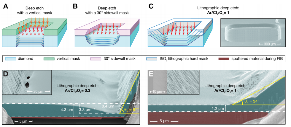
Fabrication Method: The authors present a "lithographic deep etch" (LDE) process that allows the creation of homogeneous, thin (down to 70 nm) diamond membranes. The technique uses a SiO₂ mask, coupled with alternating Ar/Cl₂ and O₂ plasmas, to achieve precise control over etching and minimize the formation of trenches or thickness gradients.
Surface Quality: The resulting diamond membranes exhibit atomically smooth surfaces, with roughness (Rq) as low as 200 pm, which is essential for maintaining high coherence in quantum devices. The process also ensures contamination-free surfaces, which is crucial for applications like hosting spin defects in diamond (e.g., nitrogen-vacancy centers).
Large-Scale Fabrication: The LDE method enables the production of large, free-standing nanostructures (up to millimeter scales), such as photonic crystal cavities and waveguides, with high uniformity. These structures are compatible with pick-and-place transfer techniques, making them suitable for integration with heterogeneous quantum systems.
Quantum Device Application: The fabrication process is applied to create nanostructures such as waveguides with distributed Bragg reflectors (DBRs) and photonic crystal cavities, optimized for wavelengths around 1042 nm, which aligns with the nitrogen-vacancy center's emission. These structures are critical for the development of efficient, scalable quantum photonic devices.
Advancements in Diamond Processing: The article also introduces an innovative approach to optical lithography for defining patterns on the diamond surface. This method, using direct laser writing (DLW), significantly enhances the resolution and scalability of diamond microstructures, providing a promising path for high-performance quantum devices.
In summary, the study highlights a scalable, efficient, and precise fabrication technique for creating diamond-based nanostructures with excellent surface quality, which are crucial for next-generation quantum technologies.
OMeda (Shanghai Omedasemi Co.,Ltd) was founded in 2021 by 3 doctors with more than 10 years of experience in nanpfabrication. It currently has 15 employees and has rich experience in nanofabrication (coating, lithography, etching, two-photon printing, bonding) and other processes. We support nanofabrication of 4/6/8-inch wafers.