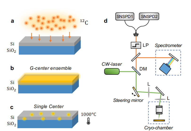
The article focuses on the scalable manufacturing of quantum light emitters in silicon, specifically using rapid thermal annealing to form single color centers. These quantum light sources, such as silicon-based color centers, are crucial for quantum technologies like networking, sensing, and computation. The fabrication process involves carbon implantation into silicon, followed by rapid thermal annealing. The study investigates how annealing affects the density and optical properties of the color centers.
Key findings include:
Annealing Time Dependency: The density of single color centers decreases exponentially with increased annealing time, while the inhomogeneous broadening of the emitted light dramatically changes, potentially reducing by up to three times compared to current methods. This is due to nanoscale thermal processes during annealing that induce local strain fluctuations around the centers.
Role of Rapid Thermal Annealing: Annealing is essential for forming single centers with high signal-to-background ratios but also introduces challenges. Longer annealing times lead to a broader zero-phonon line (ZPL) and decrease the density of single centers due to defect creation and carbon diffusion.
Microscopic Effects: First-principles calculations reveal that annealing induces strain variations around the G-centers, which affects the optical properties, including the observed blue shift and broadening of the ZPL.
Implications for Scalability: While rapid thermal annealing is critical for the creation of high-quality color centers, it currently limits the scalability of their manufacturing. Optimizing annealing time and reducing the dependence on annealing could improve scalability.
This research highlights the balance needed between annealing for defect repair and controlling the material properties for scalable quantum emitter fabrication.
OMeda (Shanghai Omedasemi Co.,Ltd) was founded in 2021 by 3 doctors with more than 10 years of experience in nanpfabrication. It currently has 15 employees and has rich experience in nanofabrication (coating, lithography, etching, two-photon printing, bonding) and other processes. We support nanofabrication of 4/6/8-inch wafers.