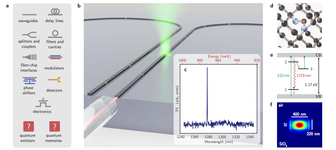
The article demonstrates the integration of G-center artificial atoms in silicon photonic integrated circuits (PICs) and their ability to be individually addressed and spectrally programmed. These G-centers, a type of carbon-related color center in silicon, emit photons at a telecommunications O-band wavelength (1278 nm), making them ideal for quantum technologies, especially in communication and processing tasks that require integration with existing silicon photonics technology.
Integration of G-centers in SOI:
The team successfully incorporated G-centers into silicon-on-insulator (SOI) photonic waveguides, enabling single-photon emission that can be efficiently coupled into the waveguides. This marks a significant step toward scalable quantum photonics, as silicon photonics provides a mature and compatible platform for integration.
Spectral Properties:
The G-centers exhibit a zero-phonon line (ZPL) transition at 1278 nm, with an inhomogeneous spectral distribution having a narrow standard deviation of 1.1 nm. This narrow spectral range is an improvement over previous reports, making them suitable for integration into fiber-optic communication systems using the O-band.
Single-Photon Emission:
Autocorrelation measurements using Hanbury-Brown-Twiss interferometry confirmed single-photon emission from the G-centers, with a second-order correlation g(2)(0) = 0.38 ± 0.08, which is characteristic of single-photon emitters.
Lifetime Measurements:
The excited-state lifetime of the emitters was measured to be 8.33 ns, which is consistent with results for G-center ensembles in bulk silicon. This stable lifetime is critical for maintaining coherence in quantum systems.
Spectral Trimming and Deactivation:
A novel technique for spectral trimming using optical irradiation was demonstrated. This method allows the spectral alignment of emitters to standard 25 GHz telecom channels. Spectral shifts of up to 300 pm (55 GHz) were achieved, which is sufficient for aligning emitters to telecom grids, thereby enhancing the ability to integrate multiple emitters into a photonic system.
Additionally, the technique can be used to deactivate individual artificial atoms, allowing precise control over the presence of emitters in a specific region.
Challenges and Future Work:
The integration of G-centers in SOI waveguides showed high stability over time, with the emission not degrading after over a month of operation. However, the low collection efficiency and excitation power limitations in the current setup remain challenges for improving performance.
The study proposes further work to investigate the physics behind spectral trimming, including better resolution spectroscopy and testing with different geometries or crystal purities, to increase the range of spectral programming.
This work demonstrates the potential of using G-center artificial atoms in silicon photonics for scalable quantum technologies. The ability to address, tune, and deactivate individual quantum emitters in integrated circuits provides a new approach for building quantum photonic systems. With further improvements in system efficiency and understanding the underlying mechanisms of spectral trimming, this technique could significantly advance the development of large-scale, integrated quantum information processing platforms.
OMeda (Shanghai Omedasemi Co.,Ltd) was founded in 2021 by 3 doctors with more than 10 years of experience in nanpfabrication. It currently has 15 employees and has rich experience in nanofabrication (coating, lithography, etching, two-photon printing, bonding) and other processes. We support nanofabrication of 4/6/8-inch wafers.