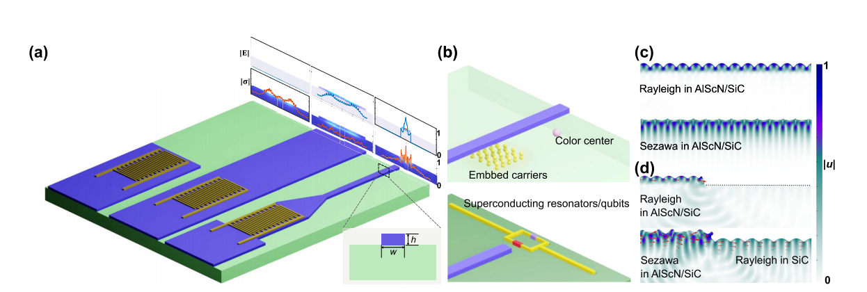
This paper introduces a new monolithic platform using AlScN (Aluminum Scandium Nitride) on SiC (Silicon Carbide) for phononic waveguides, which are promising for both acoustoelectric (AE) and quantum technologies. The AlScN/SiC platform allows for the generation and guiding of phonons at gigahertz frequencies with strong electromechanical coupling, enabling more efficient devices. The authors focus on two main modes: the Rayleigh-like mode at 2.95 GHz and the Sezawa-like mode at 4.05 GHz. These modes are characterized by high electromechanical coupling coefficients (k2 = 4.27% for Sezawa and k2 = 0.2% for Rayleigh) and propagation losses on the order of 10 dB/mm, which are suitable for phononic routing, AE amplifiers, mixers, and oscillators.
The research demonstrates that Sezawa-like modes have the potential for stronger interactions with embedded spins in SiC, making them particularly advantageous for quantum applications involving color centers and superconducting qubits. Additionally, the AlScN/SiC platform stands out in terms of electromechanical coupling and mode velocity, offering improved performance over traditional platforms like LiNbO₃.
Through the design and fabrication of integrated phononic waveguides, including the use of impedance-matched interdigital transducers (IDTs), the study shows reduced power dissipation and enhanced nonlinearities for AE devices. The findings highlight the platform’s potential for scalable, high-efficiency AE devices and its significant role in quantum information processing applications. The research also explores spin-strain coupling, demonstrating that Sezawa-like phonons exhibit stronger spin–strain coupling to SiC’s divacancy centers, which is crucial for quantum spin-based technologies.
In conclusion, the AlScN/SiC platform provides an excellent solution for efficient AE waveguides and serves as a promising basis for future phononic devices in classical and quantum applications.
OMeda (Shanghai Omedasemi Co.,Ltd) was founded in 2021 by 3 doctors with more than 10 years of experience in nanpfabrication. It currently has 15 employees and has rich experience in nanofabrication (coating, lithography, etching, two-photon printing, bonding) and other processes. We support nanofabrication of 4/6/8-inch wafers.