This paper discusses the advancements and challenges in Die-to-Wafer (D2W) hybrid and fusion bonding, particularly for chiplet heterogeneous integration. The goal is to address the issues related to tool integration, yield, placement accuracy, and metrology during the transition of D2W bonding from low-volume to high-volume manufacturing (HVM), particularly for applications like high-bandwidth memory (HBM) and CMOS image sensors (CIS).
D2W Hybrid Bonding Challenges:
Yield & Placement Accuracy: As chiplet packaging moves toward higher I/O density, challenges arise in keeping the die placement accurate as pitch scales down, with the requirement of high precision for bonding at sub-micron scales.
Metrology: Traditional optical methods for overlay inspection (used in Wafer-to-Wafer bonding) are insufficient for D2W bonding, necessitating more advanced approaches.
TEL Clean Carrier (TCC):
The TCC is a new carrier designed to mitigate contamination issues that arise from the use of traditional tape frame carriers. The TCC ensures cleaner die handling and better yield by preventing organic contamination during the bonding process.
It is compatible with existing platforms for surface preparation and bonding, without needing to scale up chambers designed for tape frames.
Process Integration:
The TCC integrates with a cluster tool, which handles surface preparation, D2W bonding, and optional onboard metrology. This streamlines the process and ensures that each die is handled optimally during the bonding steps.
The TCC also allows for die ejection and placement accuracy in handling various die sizes and thicknesses, particularly for high-performance applications like HBM.
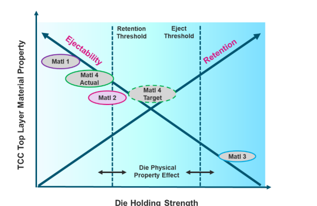
Die Handling and Retention:
The TCC is designed to securely hold dies during surface preparation steps while ensuring easy die ejection. A critical element is ensuring that the die retention strength is not too low (which could cause the die to detach) or too high (which could prevent successful die ejection).
Overlay Metrology and Placement Accuracy:
For D2W bonding, achieving placement accuracy in the range of 50 nm is necessary. This will require highly precise mechatronics, vision systems, and optimized fiducial designs. The goal is to push placement accuracy from the current 200 nm to 100 nm and eventually 50 nm.
The paper emphasizes the importance of overlay correction algorithms that have been highly developed for lithography but are now being adapted for D2W bonding.
X-Ray-Based Overlay Metrology:
The paper introduces x-ray metrology as a promising method for overlay measurement in D2W bonding. Traditional IR-based methods have limitations due to the inability to penetrate metal and doped Si. In contrast, x-ray imaging with Moire fiducials can provide higher resolution measurements, making it ideal for HBM die stacking.
Representative Bonding Results:
Die stacking: The work discusses stacking ultra-thin dies (down to 30 µm) and stacking up to 8 dies high for HBM applications. Some systematic voiding was observed, indicating that further process optimization is needed.
Patterned Test Vehicles (TV): Various test vehicles with 4.5 µm and 3.0 µm bond pad pitches were developed to test bonding processes. These tests show void-free bonding and suggest that the process is scalable for fine-pitch applications.
Yield Considerations:
Contamination from saw dicing was noted to cause voids at the die edges. The TCC approach helps mitigate these contamination risks, but plasma dicing is expected to be crucial for further improving yield.
The paper presents the TEL Clean Carrier (TCC) as a significant advancement in Die-to-Wafer bonding, addressing key challenges in contamination, die handling, and placement accuracy. With x-ray-based overlay metrology and ongoing improvements in the cluster tool platform, the paper lays the groundwork for future developments in high-density chiplet integration and fine-pitch die bonding.
OMeda (Shanghai Omedasemi Co.,Ltd) was founded in 2021 by 3 doctors with more than 10 years of experience in nanpfabrication. It currently has 15 employees and has rich experience in nanofabrication (coating, lithography, etching, two-photon printing, bonding) and other processes. We support nanofabrication of 4/6/8-inch wafers.