This paper explores the Chip-to-Wafer (C2W) hybrid bonding process for fine-pitch, high-density heterogeneous applications, specifically targeting Cu-to-Cu bonding for interconnects at 12 µm pitch and below. It focuses on critical process steps and evaluates the bonding technology, including wafer dicing, plasma cleaning, and post-bonding annealing.
Chip-to-Wafer Hybrid Bonding:
Challenges: The need for high interconnect density, ultra-fine pitch, and low-temperature bonding. The paper highlights the difficulties of achieving strong bonding interfaces with minimal voids, especially in fine-pitch applications.
Cu-Cu Bonding: The study investigates Cu-to-Cu hybrid bonding as a promising solution for high-density interconnects in applications like 2.5D and 3D packaging.
Process Flow and Methodology:
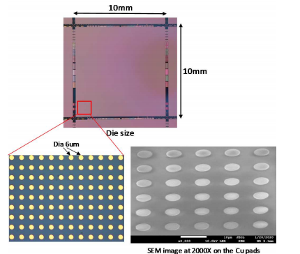
The chip, with a 6 µm Cu pad and 12 µm pad pitch, is used in the hybrid bonding process.
Key steps in the process include wafer dicing, plasma cleaning, bonding, and post-bonding annealing at 300°C for 2 hours.
Bonding Parameters: Bond force (20N to 50N), bond time (30 to 90 seconds), and post-annealing temperature (200°C and 300°C) were varied to evaluate process optimization.
Surface Activation: Plasma treatments using gases like nitrogen, oxygen, and hydrogen were used to improve surface wettability before bonding .
Wafer Dicing and Surface Preparation:
Dicing Process: The paper investigates the mechanical dicing method, which aims to reduce die chipping and minimize silicon dust. Results show minimal die chipping and particle contamination after the dicing process.
Surface Cleaning: Plasma cleaning steps ensure that die surfaces are clean and ready for bonding, which is critical to prevent bonding defects like voids.
Plasma Treatment:
Plasma treatment plays a crucial role in improving surface wettability and cleaning the Cu and thermal oxide surfaces. Oxygen, nitrogen, and hydrogen plasma were tested at different power levels and times.
The results show that higher plasma power and longer exposure times reduce contact angles, making the surfaces more hydrophilic.
Bonding Results:
Cu-Cu Bonding: The hybrid bonding achieved Cu-to-Cu bonding accuracy within ±2 µm. However, some bonding defects were observed, including small gaps between the Cu pads and the thermal oxide interface, which impacted yield.
The study also evaluated the impact of bonding force on quality. A higher force (100N) provided better bonding strength, with a shear strength of 21.5 MPa at 100N, compared to lower forces.
The best results for bonding yield were seen in oxide-to-oxide bonding, with a yield of 87.7% for 188 dies bonded onto a 12-inch oxide wafer.
Summary and Conclusions:
Plasma treatments (oxygen, nitrogen) reduce the contact angle without damaging the passivation layer, improving the bonding quality.
Hydrogen plasma effectively removes the Cu oxide layer, crucial for strong Cu-to-Cu bonding.
Cu dishing (~5 nm) is required for successful Cu-to-Cu interconnects.
Bonding accuracy was achieved within ±2 µm, showing the potential for ultra-fine pitch applications.
The paper demonstrates that hybrid bonding, particularly Cu-to-Cu bonding, is viable for fine-pitch interconnects down to 12 µm and potentially below. Key factors influencing bonding quality include surface preparation, plasma treatment, and bonding parameters.
Key Findings:
The study was supported by the Science and Engineering Research Council of A*STAR, Singapore, and various contributors to the project.
OMeda (Shanghai Omedasemi Co.,Ltd) was founded in 2021 by 3 doctors with more than 10 years of experience in nanpfabrication. It currently has 15 employees and has rich experience in nanofabrication (coating, lithography, etching, two-photon printing, bonding) and other processes. We support nanofabrication of 4/6/8-inch wafers.