The article Assembly Perspectives on Flip-Chip Integration of 1x, 4x, and 8x Array InP-SiN Hybrid Laser Devices to Si Photonics Wafers with Sub-500 nm Misalignment explores the assembly and integration process of InP-based hybrid laser devices onto silicon photonics (SiPho) wafers, focusing on the scaling from single-channel to multi-channel arrays and achieving precise alignment during the flip-chip bonding process.
Key findings from the article include:
Flip-Chip Bonding Process: The paper discusses the use of laser-assisted bonding for high-precision flip-chip integration, utilizing the ASMPT AMICRA NANO tool. This method ensures sub-micron placement accuracy and involves four main steps: die-substrate alignment, placement, laser-assisted bonding, and post-bond misalignment measurement. The process aims to minimize misalignment, ensuring good coupling between laser outputs and SiPho waveguides, which is crucial for device performance.
Scaling to Multi-Channel Devices: The study focuses on three types of devices: single-channel (1x), four-channel (4x), and eight-channel (8x) InP lasers. These devices were integrated using the same basic alignment and bonding procedures, with slight variations in the process for scaling up to larger arrays. The challenge with larger arrays is maintaining alignment across multiple channels to avoid coupling losses.
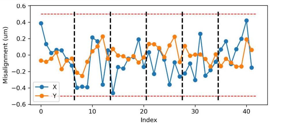
Alignment and Misalignment: Achieving precise alignment is critical, especially for multi-channel devices. The article discusses the interaction between the bonding tool, device, and landing site, as well as how rotational and XY misalignment can affect device performance. Misalignments in both directions were kept below 500 nm for most devices, with average misalignments of 183 nm in X and 89 nm in Y for 1x devices. However, slight misalignment increases with larger arrays, with rotational shifts contributing to channel misalignment.
Post-Bond Measurements: Post-bond misalignment measurements showed that the bonding process achieved an average absolute misalignment of 250 nm and rotational misalignment below 0.05°, with some slight bowing and tilting effects. These effects were more prominent in larger arrays (4x and 8x), which showed a maximum tilt of ~150 nm, but they had minimal impact on the coupled power for devices within the bonding tolerances.
Device Performance: Despite the misalignment, the power output of the devices remained consistent across all channels. The coupling losses were found to be less significant for misalignments in the X direction compared to the Y direction, particularly in devices with rotational misalignment. The results showed that proper alignment is crucial for optimal coupling and minimal power loss.
Conclusion: The study concluded that while larger multi-channel devices require stricter alignment specifications, particularly in rotational alignment, high-quality bonding techniques can maintain excellent performance even for 8-channel devices. It also highlighted the importance of careful handling and bonding tool design to manage device warpage and bowing, especially for larger arrays.
In summary, the paper presents a thorough examination of the flip-chip bonding process for InP-SiN hybrid laser devices, showcasing the ability to scale from single-channel to multi-channel devices while maintaining precise alignment and low coupling losses .
OMeda (Shanghai Omedasemi Co.,Ltd) was founded in 2021 by 3 doctors with more than 10 years of experience in nanpfabrication. It currently has 15 employees and has rich experience in nanofabrication (coating, lithography, etching, two-photon printing, bonding) and other processes. We support nanofabrication of 4/6/8-inch wafers.