Paper Download
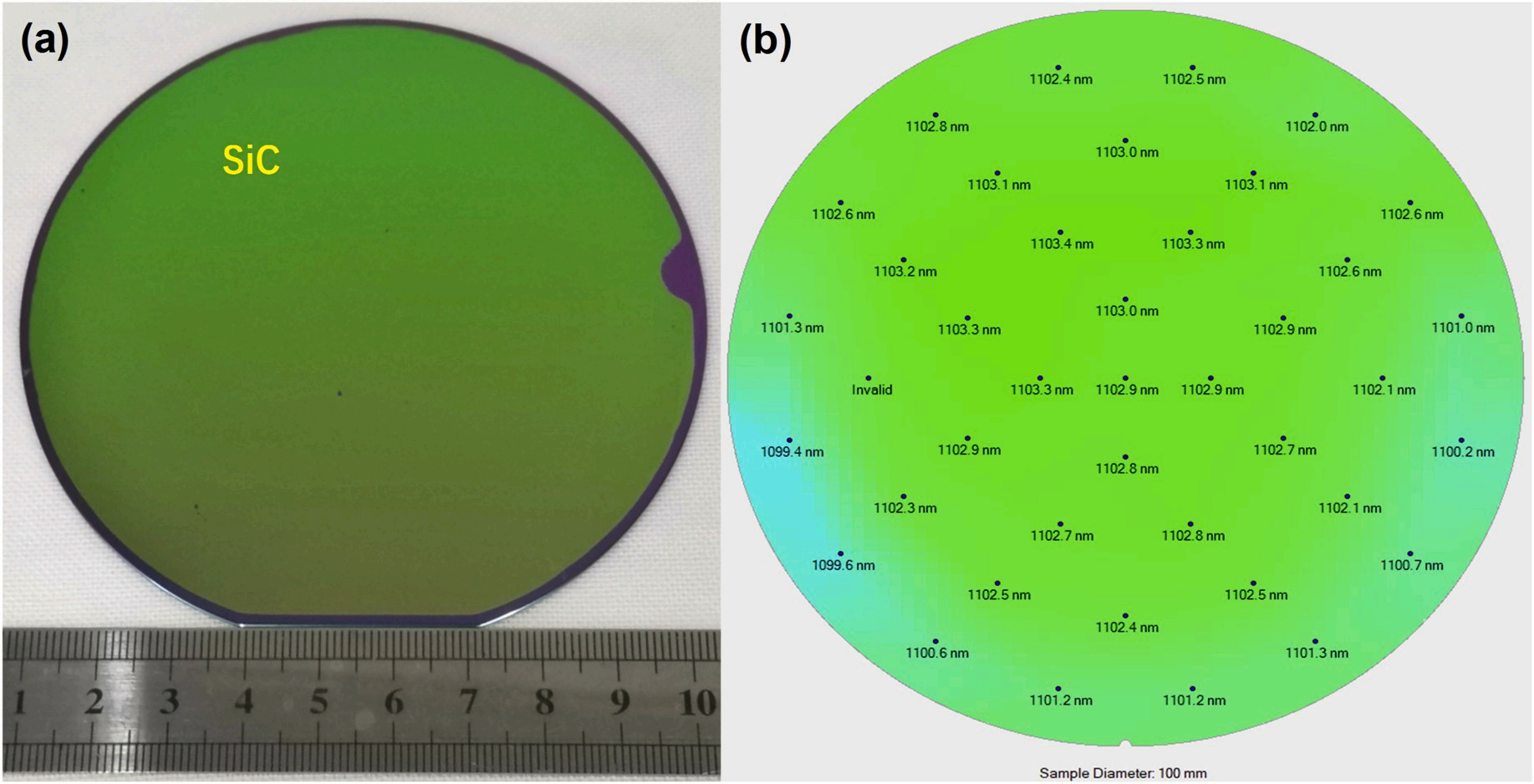
We provide 4-6 inch SICOI wafers (silicon carbide on insulator wafers). The wafers use surface activated bonding technology to bond thermal oxide wafers and 4H high-purity semi-insulating silicon carbide wafers together, and then control the thickness to the thickness you need through ion implantation, annealing, thinning or direct thinning and CMP polishing. It is worth noting that ion implantation and direct CMP and thinning have their own advantages and disadvantages.we also have many stock ,you can visit this page to know more : SICOI Wafer( Silicon Carbide on Insualtor)
The article titled **"Wafer-scale 4H-Silicon Carbide-on-Insulator (4H-SiCOI) Platform for Nonlinear Integrated Optical Devices"** explores the development and fabrication of 4H-silicon carbide (SiC) films on a silicon substrate, using ion-cutting and layer transfer techniques for nonlinear integrated optical applications. Here’s a summary of the key points:

1. **Material and Platform:** The study demonstrates the successful fabrication of a wafer-scale 4H-SiCOI platform, which offers high-quality, single-crystalline 4H-SiC films on a Si (100) substrate with an intermediate SiO₂ layer. This platform is highly suitable for nonlinear optical and quantum photonic applications due to the desirable material properties of 4H-SiC, such as its large bandgap, high thermal conductivity, and significant nonlinear optical properties.
2. **Fabrication Process:**
- The 4H-SiC films were fabricated using an ion-cutting and layer transfer technique, similar to methods used in mass production of silicon-on-insulator (SOI) wafers.
- Hydrogen ions were implanted into the 4H-SiC wafer to create a damaged layer, followed by bonding the wafer to a SiO₂/Si substrate. A subsequent annealing process enabled the transfer of the SiC layer to the Si substrate.
3. **Thermodynamics of Surface Blistering:** The study explored the conditions for blister formation on the 4H-SiC surface due to hydrogen ion implantation. A critical temperature for blister formation was determined to be around 800°C, and the mechanism of blister growth was modeled based on thermodynamic principles.
4. **Micro-ring Resonators:** The researchers fabricated micro-ring resonators on the 4H-SiCOI platform with a quality factor (Q) of up to 66,000 for transverse electric (TE) modes. These resonators demonstrate the platform’s potential for integration into optical devices for telecom applications and nonlinear photonics.
5. **Results and Characterization:**
- **X-ray Diffraction (XRD):** The single-crystalline quality of the transferred SiC films was confirmed using XRD measurements, with a full width at half maximum (FWHM) of 75.6 arcsec after annealing.
- **Atomic Force Microscopy (AFM):** The surface roughness of the SiC film was reduced to 0.5 nm through chemical mechanical polishing (CMP), confirming the smoothness needed for high-performance optical devices.
- **Transmission Electron Microscopy (TEM):** High-resolution TEM images confirmed the single-crystalline nature of the 4H-SiC films, with minimal defects after annealing and CMP.
6. **Conclusion:** The wafer-scale 4H-SiCOI platform offers a promising solution for nonlinear integrated optical devices due to its high-quality crystalline SiC film, which can be further improved by optimizing the ion implantation and post-annealing processes. This platform has the potential for applications in optical resonators, quantum photonics, and nonlinear optics.
This study presents significant advancements in the integration of SiC films for photonic applications, paving the way for large-scale production and improved device performance.
OMeda (Shanghai Omedasemi Co.,Ltd) was founded in 2021 by 3 doctors with more than 10 years of experience in nanpfabrication. It currently has 15 employees and has rich experience in nanofabrication (coating, lithography, etching, two-photon printing, bonding) and other processes. We support nanofabrication of 4/6/8-inch wafers.