Paper Download
OMedaSemi use SAB Bonding Methond to bonding most of material,Surface activated bonding (SAB) is a room temperature wafer bonding technique with an atomically cleaned and activated surface. Surface activation is usually performed prior to bonding using rapid atomic bombardment to clean the surface. High strength bonds between semiconductors, metals, and dielectrics can be obtained even at room temperature.This bonding method can bond most of material ,such as Diamond, Sic,GaN,LiNbO3,Glass,Silicon,Sapphire,Inp,GaAs. if you want to know more ,please visit this page:Surface Actived Bonding Technology
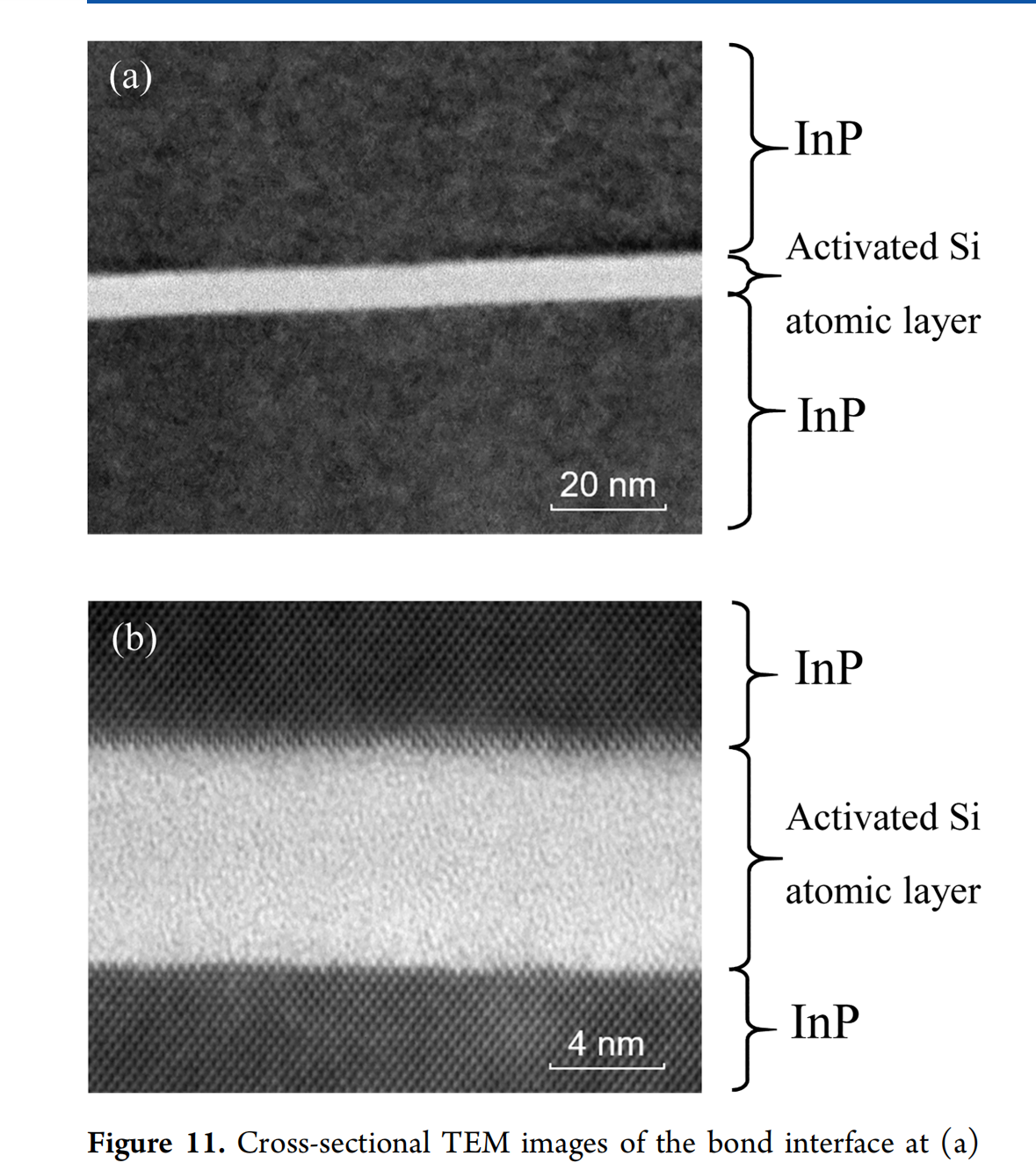
The article "Room-Temperature Bonding of Indium Phosphide Wafers and Their Atomic Structure at the Bond Interface" investigates two bonding methods for indium phosphide (InP) wafers at room temperature: Surface-Activated Bonding (SAB) and bonding using an activated silicon (Si) atomic layer.

Surface-Activated Bonding (SAB):
SAB involves irradiating wafer surfaces with an argon fast atomic beam (Ar FAB) to remove contaminants and activate bonding surfaces.
This method results in increased surface roughness and weaker bond strength for InP compared to other materials like silicon (Si), due to the formation of a damaged layer and In-rich surface.
The bond strength achieved through SAB was found to be relatively low at 0.4 J/m², insufficient for further processing like wafer polishing.
Activated Si Atomic Layer Bonding:
This method avoids direct irradiation of InP wafers and uses sputtered Si atoms to create an intermediate Si layer for bonding.
The activated Si layer results in smoother surfaces and stronger bonds (0.9 J/m²), more than twice as strong as SAB.
The diffusion of indium (In) and phosphorus (P) into the Si layer suggests that this method is not simply bonding two Si bulks but involves material interaction between the InP and Si atomic layers.
Applications and Conclusion:
The study provides insights into the atomic structure of the bond interface and the surface morphology after different bonding processes.
It concludes that bonding using the Si atomic layer shows superior bond strength and surface quality, making it a promising technique for the integration of InP-based electronics and photonics.
This research advances the understanding of room-temperature bonding for semiconductor materials, crucial for heterogeneous integration of materials with different properties.
OMeda (Shanghai Omedasemi Co.,Ltd) was founded in 2021 by 3 doctors with more than 10 years of experience in nanpfabrication. It currently has 15 employees and has rich experience in nanofabrication (coating, lithography, etching, two-photon printing, bonding) and other processes. We support nanofabrication of 4/6/8-inch wafers.