Paper Download

This article investigates the enhancement of the electro-optic (EO) response in 150-nm-thick BaTiO₃ (BTO) films integrated on Si through controlling heating and cooling rates during molecular beam epitaxy (MBE) growth.
Silicon photonics (SiPh) demands materials with strong EO responses, and BTO is promising due to its large EO response and compatibility with CMOS fabrication, outperforming LiNbO₃ (LNO) which has modest EO response and CMOS contamination issues.
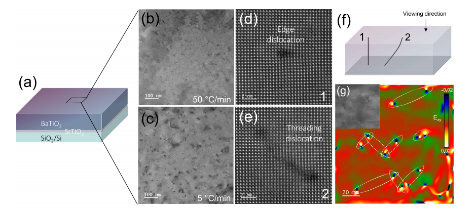
The study varied cooling rates (50, 10, and 5 °C/min) and characterized the films using X-ray diffraction (XRD), scanning transmission electron microscopy (STEM) with precession electron diffraction, and EO measurements. Key findings include:
- Contrary to previous reports, faster cooling (50 °C/min) resulted in more c-axis oriented BTO, while slower cooling (5, 10 °C/min) led to more a-axis oriented regions with greater relaxation, possibly due to dominant electrostatic boundary conditions in thicker films.
- Crystallographic domain sizes (≈50–100 nm) and defect densities were similar across different cooling rates, though relaxation degrees varied consistent with XRD results.
- The effective Pockels coefficients exceeded 550 pm/V, and after accounting for a-axis equivalent thickness, the effective EO responses were comparable across samples, indicating negligible dependence on lattice relaxation or domain size beyond sufficient thickness. Raw modulation depended on a-axis BTO thickness.
Conclusions highlight that cooling rates control a-axis BTO thickness, providing insights for Si-integrated photonics by demonstrating a robust BTO growth process with stable EO performance post-sufficient relaxation.
OMeda (Shanghai Omedasemi Co.,Ltd) was founded in 2021 by 3 doctors with more than 10 years of experience in nanpfabrication. It currently has 15 employees and has rich experience in nanofabrication (coating, lithography, etching, two-photon printing, bonding) and other processes. We support nanofabrication of 4/6/8-inch wafers.