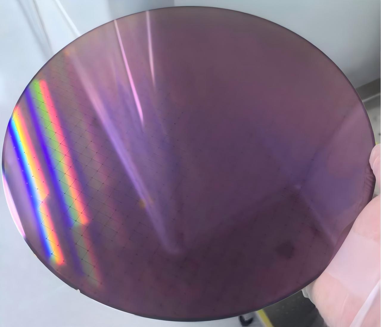
OMedaSemi provides a complete hybrid bonding process, from hybrid bonding wafer fabrication and plasma dicing to hybrid bonding fabrication. We use 8-inch and 12-inch EVG Gemini FB fully automated hybrid bonding equipment for hybrid bonding foundry services based on CuSiO2 and CuSiCN material systems.
Features:
* Supports 8-inch and 12-inch wafers
* Supports CuSiO2 and CuSiCN material systems
* Uses EVG Gemini equipment with alignment accuracy less than 50nm
* We can perform custom processing and hybrid bonding of hybrid bonding verification wafers, TSV wafers, and TGV wafers.
Lead Time: 7 days
Reference Price: 1100 USD/pcs. Discounts available for bulk orders. Welcome cooperation from organizations or scientists with long-term needs.
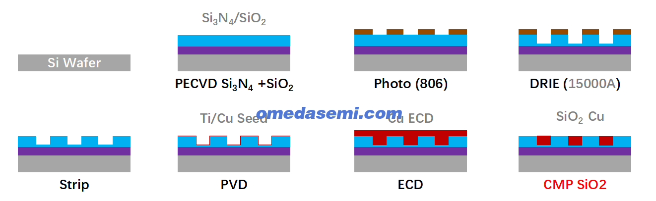
Wafer fabrication process flow:
Wafer-to-wafer hybrid bonding process flow:
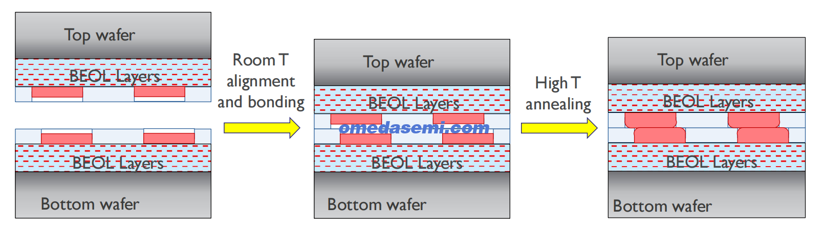
Step 1: Polish the top and bottom surfaces to an ultra-smooth finish, with a dielectric layer surface roughness of less than 0.5 nm and pad dishing less than 5 nm.
Step 2: Align the top and bottom surfaces and activate the dielectric layer material contact pre-bonding at room temperature, leaving gaps between the copper materials.
Step 3: High-temperature annealing to enhance bond strength, while Cu expands the contact, eliminating gaps.
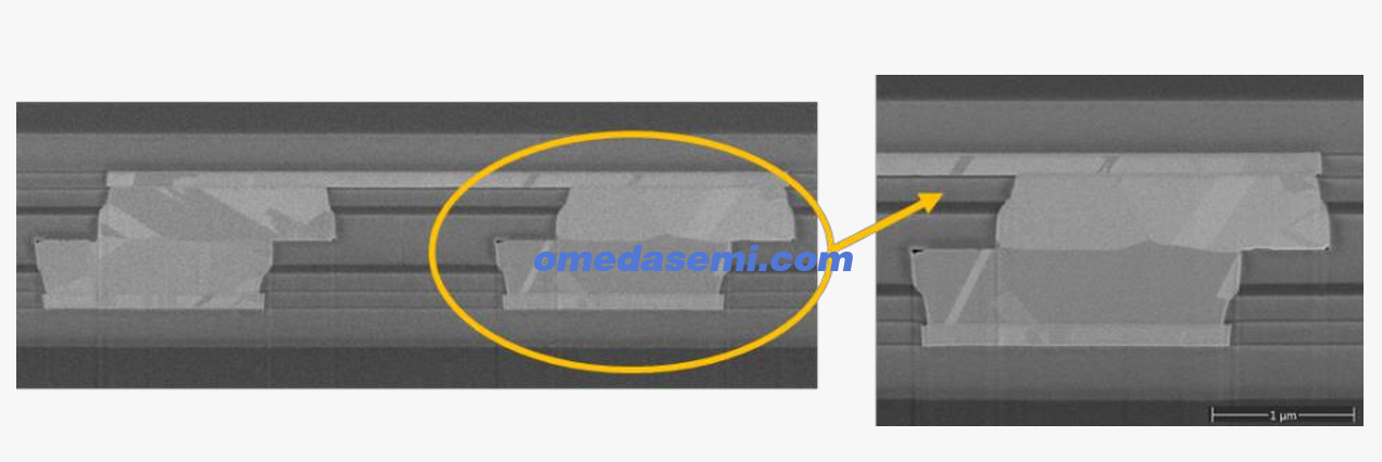
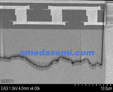
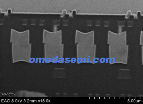
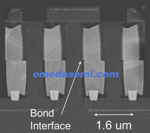
Bonding results shown:
OMeda (Shanghai Omedasemi Co.,Ltd) was founded in 2021 by 3 doctors with more than 10 years of experience in nanpfabrication. It currently has 15 employees and has rich experience in nanofabrication (coating, lithography, etching, two-photon printing, bonding) and other processes. We support nanofabrication of 4/6/8-inch wafers.