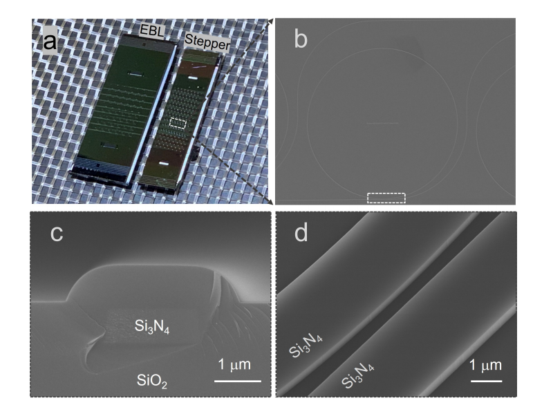
The paper discusses the fabrication of ultra-low-loss photonic integrated circuits (PICs) using an 8-inch, crack-free, dispersion-engineered Si₃N₄-SiO₂-Si wafer. The wafers are produced using a process compatible with industrial silicon photonics fabrication lines. The work highlights how a modified subtractive fabrication technique, combined with an amorphous silicon (a-Si) hardmask etching technique, results in Si₃N₄ PICs with intrinsic quality factors exceeding 22 × 10⁶ and a propagation loss of 1.54 dB/m.
The authors demonstrate that the fabricated Si₃N₄ waveguides exhibit anomalous dispersion, essential for applications like frequency comb generation. The study successfully demonstrates soliton frequency comb generation using an auxiliary-laser-assisted bi-pumping technique, confirming the effectiveness of the designed anomalous dispersion in the waveguides.
The paper concludes that the developed fabrication process for Si₃N₄ PICs is robust, scalable, and compatible with standard silicon photonics foundry processes, opening new avenues for applications in nonlinear optics and quantum information processing.
Key outcomes include:
The fabrication of high-performance, ultra-low-loss Si₃N₄ PICs using standard industrial fabrication methods.
Successful generation of soliton frequency combs on the fabricated devices.
The demonstration of anomalous dispersion critical for nonlinear optical applications.
A highly reproducible and reliable fabrication process for mass production on large wafers (8 inches or larger), ensuring scalability for practical applications in quantum optics and telecommunications.
These advances address challenges in the mass production of Si₃N₄-based devices, paving the way for cost-effective, high-yield manufacturing for optical communication, nonlinear optics, and quantum technologies.
OMeda (Shanghai Omedasemi Co.,Ltd) was founded in 2021 by 3 doctors with more than 10 years of experience in nanpfabrication. It currently has 15 employees and has rich experience in nanofabrication (coating, lithography, etching, two-photon printing, bonding) and other processes. We support nanofabrication of 4/6/8-inch wafers.