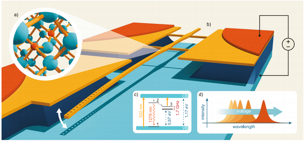
The article discusses the precise control of spectral tuning and nanoscale localization of single G-centers in silicon, with a focus on integrating these color centers into photonic circuits for scalable quantum technologies. The work demonstrates the use of a microelectromechanical system (MEMS) cantilever to apply strain to silicon waveguides, which results in reversible spectral tuning of individual G-centers. This tuning method enables precise control over the optical transitions of the emitters, crucial for quantum networking applications.
Key points from the paper:
Strain-Induced Spectral Tuning: The MEMS cantilever applies strain to silicon waveguides to shift the emission wavelength of G-centers. A voltage difference of up to 35 V induces a shift of over 100 pm without affecting brightness. This method allows for the fine-tuning of individual emitters' optical transitions, making them more suitable for large-scale integration in quantum systems.
Modeling and Nanoscale Localization: The spectral shifts induced by strain are modeled using a piezospectroscopic model. This model enables the extraction of the vertical position and orientation of each color center within the waveguide with sub-3 nm precision. The spatial positioning, dipole orientation, and spectral behavior of the color centers are all correlated, providing an accurate localization of the emitters at the nanoscale.
Fabrication Process: The device is fabricated using silicon-on-insulator (SOI) wafers, carbon ion implantation to form G-centers, and MEMS-based actuation. The MEMS cantilever is patterned with photonic components including a Bragg reflector and edge coupler for efficient light collection. The fabrication process is compatible with standard photonics foundries.
Experimental Results: The team demonstrates the spectral tuning of individual G-centers in a photonic integrated circuit (PIC). The tuning is achieved by applying low-power strain to the cantilever, with the spectral shift recorded as a function of applied voltage. The results show a maximum tuning of 130 pm with a spectral tuning rate of 680 MHz/V, and up to 5.8 GHz/V under optimal conditions.
Single-Photon Emission and Correlation: The spectral properties of the G-centers were investigated through second-order correlation functions, confirming the single-photon nature of the emission. The measured second-order correlation function (g(2)(0) = 0.09 ± 0.04) demonstrates that the emitters can act as single-photon sources, a key requirement for quantum networking.
Applications and Future Work: The ability to locally tune the emission spectra and precisely localize color centers opens up opportunities for scalable quantum networks. The research lays the foundation for on-demand emitter generation and coherent coupling between remote emitters. Future improvements in device design, such as increasing the strain capabilities, could further enhance the alignment of multiple emitters within a single device and across devices.
In conclusion, this study provides a powerful method for controlling the emission properties of color centers in silicon, making it a significant step toward scalable quantum networks based on silicon photonics.
OMeda (Shanghai Omedasemi Co.,Ltd) was founded in 2021 by 3 doctors with more than 10 years of experience in nanpfabrication. It currently has 15 employees and has rich experience in nanofabrication (coating, lithography, etching, two-photon printing, bonding) and other processes. We support nanofabrication of 4/6/8-inch wafers.