The article explores the electrical manipulation of silicon color centers, specifically G centers, integrated into lateral p-n diodes on a silicon-on-insulator (SOI) wafer. This research focuses on the ability to control the optical properties of an ensemble of G centers by applying a reverse-biased electric field, which modulates the fluorescence and induces a redshift in the zero phonon line (ZPL) of the emitters.
Key findings include:
Electrical Modulation: The fluorescence intensity of the G center ensemble decreases with increasing reverse bias, while the ZPL shifts by 100 GHz at a rate of approximately 1.24 ± 0.08 GHz/V above a certain threshold voltage.
Field Distribution: The study also investigates the spatial distribution of the electric field across the junction. By imaging the electric field dynamics and correlating it with the fluorescence response, the research maps the depletion region and its impact on the emitters. The G center fluorescence shows stronger modulation and redshift in the regions closer to the n-type contact.
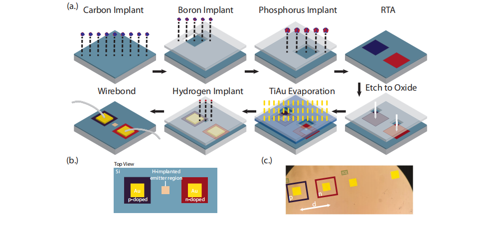
Hydrogen Role: Hydrogen implantation is crucial for the formation of G centers, with the ensemble localized in the hydrogen-implanted region, demonstrating how this process stabilizes the G centers and contributes to their optical behavior under electrical control.
Charge State Modulation: The paper suggests that the observed modulation in fluorescence and redshift can be attributed to both Stark effects (due to the electric field) and charge state changes of the G centers as a result of Fermi level engineering. These processes show how the G centers can be electrically tuned, transitioning between optically active and inactive states.
The results highlight the potential for using electrical tuning to manipulate semiconductor quantum emitters, which could be valuable for future quantum networking and photonic applications. Additionally, the study provides a tool for further exploring the electric field dynamics within semiconductors and their effects on color centers, with a broader applicability for similar platforms like silicon carbide.
OMeda (Shanghai Omedasemi Co.,Ltd) was founded in 2021 by 3 doctors with more than 10 years of experience in nanpfabrication. It currently has 15 employees and has rich experience in nanofabrication (coating, lithography, etching, two-photon printing, bonding) and other processes. We support nanofabrication of 4/6/8-inch wafers.