This article discusses an innovative method for optimizing the surface characteristics of silicon wafers during the backside removal process, particularly for use in three-dimensional (3D) integration. The research focuses on the challenges faced in thinning the silicon wafer for advanced semiconductor applications, where the removal of backside silicon is crucial for improving performance in 3D integration systems.
Key steps and findings include:
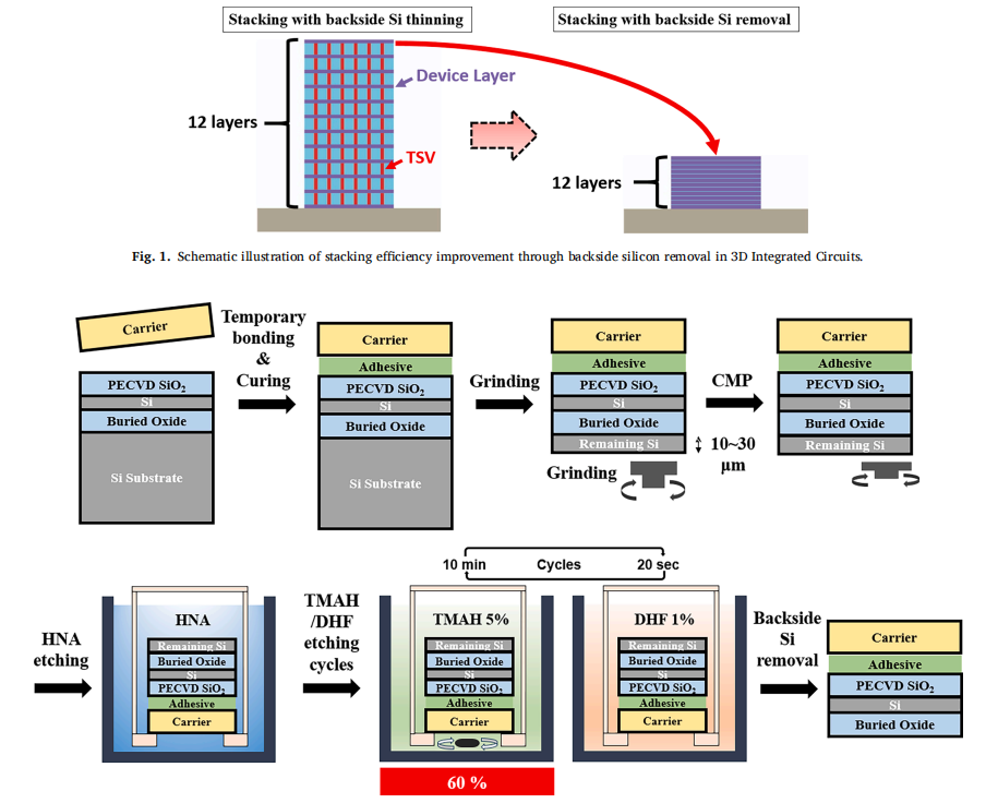
Backside Silicon Removal Process: The study details a two-stage grinding process (rough and fine) followed by Chemical Mechanical Polishing (CMP) to reduce surface roughness. After grinding, the surface stress was alleviated, and the roughness was dramatically reduced from 1 μm to 0.4 nm.
Hydrofluoric-Nitric Acid (HNA) Treatment: A treatment using HNA effectively removed non-(100) silicon layers, which is crucial for improving the etching efficiency and ensuring better surface characteristics for the subsequent etching processes.
TMAH/DHF Cycle: To enhance etching efficiency and remove native oxides, a TMAH (tetramethylammonium hydroxide) and dilute hydrofluoric acid (DHF) cycle was used. This approach not only improved the uniformity and rate of etching but also facilitated the complete removal of the backside silicon layer, exposing the buried oxide layer.
Surface Characterization: The article highlights the importance of Raman spectroscopy and Atomic Force Microscopy (AFM) in analyzing surface characteristics before and after each processing stage. Raman spectroscopy was particularly effective in detecting stress and crystallinity changes in the silicon, revealing how treatments like CMP and HNA significantly improved surface quality.
Focused Ion Beam (FIB) and X-ray Photoelectron Spectroscopy (XPS): These techniques were employed to verify the complete removal of the backside silicon. FIB imaging confirmed that the silicon was successfully removed, exposing the buried oxide layer, while XPS analysis showed the absence of silicon and confirmed the presence of only the oxide and silicon layers.
This study presents an efficient method to optimize wafer thinning processes, ensuring the high-quality removal of backside silicon while maintaining structural integrity, critical for advanced 3D integrated circuits. The findings provide valuable insights for improving surface characteristics in semiconductor manufacturing processes, leading to better performance in devices such as sensors and chips.
OMeda (Shanghai Omedasemi Co.,Ltd) was founded in 2021 by 3 doctors with more than 10 years of experience in nanpfabrication. It currently has 15 employees and has rich experience in nanofabrication (coating, lithography, etching, two-photon printing, bonding) and other processes. We support nanofabrication of 4/6/8-inch wafers.