This paper explores the integration of plasma dicing in the collective die-to-wafer hybrid bonding process, focusing on improving the reliability and precision of the hybrid bonding process. The goal is to bond dies to a target wafer using a controlled technique that minimizes defects and misalignment.
Process Overview:
Die-to-Wafer Hybrid Bonding: The process starts with fabricating wafers that have a Cu pad layer embedded in a dielectric layer (SiCN). After cleaning and preparing the dies, plasma dicing is performed to form the die.
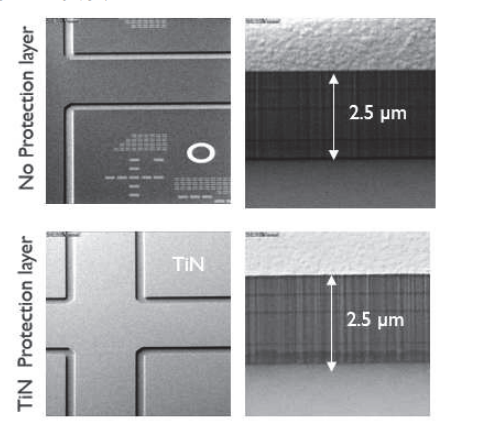
Plasma Dicing: This involves etching with a laser and applying plasma etching to achieve precise dicing of the dies into smaller chips. After this, a protective layer (e.g., TiN) is used to avoid damage to the Cu structures.
Die Placement and Cleaning: After dicing, the dies are transferred to the target wafer using a wafer-to-wafer bonding tool. The alignment of dies is measured and adjusted if necessary, ensuring accurate placement of the die onto the target wafer .
Plasma Dicing Steps:
The plasma dicing technique uses a specialized tool to etch the dies without damaging the underlying metal structures. A second step involves removing any potential residues and ensuring that the dies remain intact and properly aligned with the target wafer.
Additionally, TiN is used as a protective layer to preserve the Cu structures during the process .
Electrical Measurements:
The resulting dies were tested electrically to measure their performance. The tests included the Kelvin structure for bonding quality and the Daisy Chain structure to ensure uniformity. The effectiveness of TiN as a protective layer was measured, revealing better electrical yields in dies with this layer compared to those without .
Key Findings:
The integration of plasma dicing enhances the hybrid bonding process, with electrical yields improving significantly when using a TiN protective layer. However, defects due to the adhesive material were observed, particularly when alignment errors occurred .
The use of TiN showed higher electrical yields in Daisy Chain structures, particularly in the 5 to 7µm pitch range.
Conclusion:
Plasma dicing effectively integrates into the die-to-wafer hybrid bonding process, improving yield and performance. Further investigation into process optimization is needed, especially concerning alignment precision and the impact of different protective layers .
OMeda (Shanghai Omedasemi Co.,Ltd) was founded in 2021 by 3 doctors with more than 10 years of experience in nanpfabrication. It currently has 15 employees and has rich experience in nanofabrication (coating, lithography, etching, two-photon printing, bonding) and other processes. We support nanofabrication of 4/6/8-inch wafers.