This paper discusses the direct die-to-wafer (D2W) hybrid bonding process using plasma diced dies with bond pad pitch scaling down to 2 µm. The paper outlines the entire die preparation process, including backside thinning, plasma dicing, surface activation, and pick-and-place procedures, to minimize defects at the bonding surface and to enable the handling of thin dies.
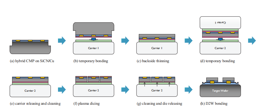
Process Flow:
The process begins with the preparation of wafers with a SiCN dielectric surface and uniform Cu patterns. Chemical-mechanical polishing (CMP) ensures surface quality, with Cu recess controlled to under 5 nm.
A series of temporary bonding steps are used to handle thin wafers, including thinning the backside to 50 µm and using laser-releasable materials to assist in transferring the dies to the target wafer.
Plasma dicing is employed to singulate the dies, achieving clean edges and enabling flexible die shape designs, such as chamfered corners, which help reduce stress at the die edges.
Design of Test Structures:
Four types of 2 µm and 3 µm bond pad designs are used to explore different geometries. The smallest pads (0.50 µm x 0.50 µm) have tight overlay accuracy requirements, while larger pads allow for greater Cu bulge-out during bonding.
Test structures include both Kelvin and interwoven daisy chains for electrical yield (e-yield) analysis.
Results:
CMP Optimization: Cu recess levels were kept below 5 nm for different pad sizes, which is crucial for achieving strong Cu-Cu bonding during post-bonding annealing.
Plasma Dicing Benefits: Plasma dicing provided clear die edges and smooth sidewalls, which helped reduce bonding voids and minimize edge-related defects .
Electrical Characterization: The electrical yield for the 3 µm pitch designs was >95% for Kelvin structures and >90% for daisy chain structures. For the 2 µm pitch design, the yields were slightly lower but still above 80% for Kelvin and 70% for daisy chains .
Challenges:
While the translation and rotation errors in the die placement were well-controlled, scaling errors due to wafer warpage remained a challenge. These issues could be addressed through better warpage control and tooling.
The paper demonstrates that direct D2W hybrid bonding using plasma diced dies with bond pad pitches down to 2 µm is feasible, with good electrical yields for both 2 µm and 3 µm test structures. Plasma dicing helps in improving die quality and bonding precision, making it suitable for high-density, fine-pitch interconnections in advanced semiconductor packaging.
OMeda (Shanghai Omedasemi Co.,Ltd) was founded in 2021 by 3 doctors with more than 10 years of experience in nanpfabrication. It currently has 15 employees and has rich experience in nanofabrication (coating, lithography, etching, two-photon printing, bonding) and other processes. We support nanofabrication of 4/6/8-inch wafers.