The article Fine-Pitch Die-to-Wafer Bonding Technologies for Chiplet Integration focuses on the development of fine-pitch interconnect technologies for integrating chiplets onto a silicon interposer. The study investigates three different bonding technologies—hybrid bonding, microbump bonding, and nanowire bonding—designed for high-performance chiplet integration with a pitch size of 10 µm. These technologies are evaluated for their effectiveness in high-performance computing (HPC) applications, where precise, high-density interconnects are required.
Chiplet and Interposer Design:
The study designs chiplets with various sizes (1x1 mm², 4x4 mm², 9x9 mm²) and interconnects with a pitch size of 10 µm, focusing on different interconnect technologies: hybrid bonding, microbump, and nanowire bonding. These chiplets are fabricated to be bonded on a silicon interposer with a Cu/SiO₂ hybrid bonding surface. The wafers are tested using redistribution layer (RDL) structures that allow electrical measurements.
Fabrication Process:
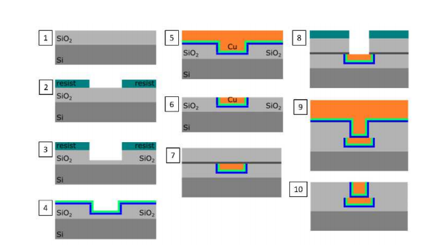
Interposer Fabrication: The process includes oxide deposition, photolithography, copper electroplating, and chemical-mechanical polishing (CMP) to create a flat and clean surface for bonding.
Chiplet Fabrication: The chiplets undergo similar processing, where after CMP, they are singulated via stealth dicing. Each chiplet is then processed for either hybrid bonding, microbump bonding, or nanowire bonding.
Nanowire Bonding: Copper nanowires are electroplated onto the pads of the chiplets for this process, which is crucial for achieving fine-pitch interconnects.
Microbump Bonding: A controlled wet etching process is used to create a topography on Cu pads, followed by electroplating solder bumps for the microbump bonding.
Bonding and Testing:
Hybrid Bonding: After singulation, the chiplets are activated and bonded using a die-to-wafer (D2W) hybrid bonding process, followed by annealing. The interconnect resistance for a single hybrid bond is measured at approximately 18 mΩ, which aligns with theoretical expectations.
Microbump Bonding: The microbump bonding process involves flux-less bonding, followed by reflow under a reducing atmosphere. The shear strength of the microbump interconnects is measured to be between 44 and 50 MPa.
Nanowire Bonding: Initial results for nanowire bonding show promising shear strength data, with values exceeding 40 MPa at an interface temperature of 190°C.
Combining Different Bonding Technologies:
The study demonstrates the feasibility of integrating chiplets with different bonding technologies (hybrid bonding and microbump bonding) on the same interposer. A careful alignment and bonding profile adjustment are necessary for successful integration. The study highlights that while hybrid bonding has more stringent surface requirements, both hybrid and microbump bonding can be successfully combined.
Challenges and Optimization:
The research emphasizes the importance of optimizing bonding processes to avoid issues such as residuals or bridging. Moreover, the correct order of bonding is critical when using multiple interconnect technologies. For example, hybrid bonding should be performed first to avoid the complete consumption of Cu pads in microbump bonding.
The study demonstrates successful integration of chiplets with different interconnect technologies on a single interposer. Hybrid bonding and microbump bonding showed the most promising results, with successful bonding without shorts or opens. The next steps include optimizing nanowire bonding technology and performing reliability tests to ensure long-term performance for high-density chiplet integration in advanced computing systems.
This work provides significant insights into the development and combination of different bonding technologies for fine-pitch, high-performance chiplet integration.
OMeda (Shanghai Omedasemi Co.,Ltd) was founded in 2021 by 3 doctors with more than 10 years of experience in nanpfabrication. It currently has 15 employees and has rich experience in nanofabrication (coating, lithography, etching, two-photon printing, bonding) and other processes. We support nanofabrication of 4/6/8-inch wafers.