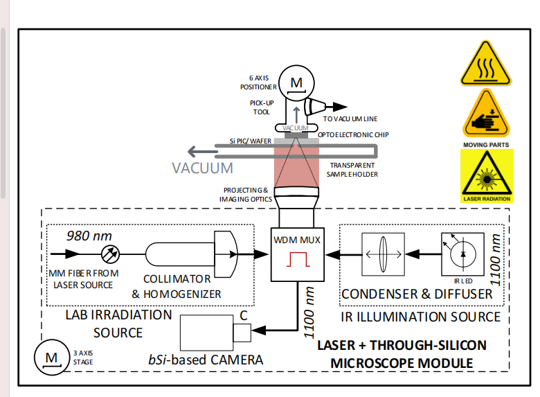
This paper discusses a novel approach for integrating a 1×1 mm multichannel III-V laser diode chip onto a silicon photonic integrated circuit using Laser-Assisted Bonding (LAB). The LAB technique overcomes the limitations of traditional bonding methods like mass-reflow and thermo-compression bonding, which often struggle with issues like poor scalability and thermal mismatch. LAB uses localized laser heating to minimize thermal stress, enhancing alignment precision to sub-micron accuracy.
A key innovation in this method is the use of a through-silicon imaging system, which allows real-time alignment and bonding. This approach enables highly accurate and repeatable bonding processes, with an experimental demonstration showing alignment accuracy of less than 0.5 µm. The results showed that the laser bonding process provided robust joint strength (13.87 N), meeting the MIL-STD-883H shear strength criteria. Additionally, the optical performance of the bonded chip demonstrated expected emission from all channels, verifying the successful integration of the laser diode chip.
The bonding process incorporates careful temperature and force control, optimized through experimentation with the solder behavior under laser irradiation. The final bonding achieved uniform bondline formation with consistent optical output from all laser channels.
The paper concludes that LAB is an energy-efficient, highly precise, and scalable method for silicon photonics integration, suitable for automated photonics packaging lines, and it holds potential for large-scale wafer-level manufacturing. The success of this technique supports its application in next-generation photonic systems, with applications in fields like communication, biomedical sensing, and imaging technologies.
OMeda (Shanghai Omedasemi Co.,Ltd) was founded in 2021 by 3 doctors with more than 10 years of experience in nanpfabrication. It currently has 15 employees and has rich experience in nanofabrication (coating, lithography, etching, two-photon printing, bonding) and other processes. We support nanofabrication of 4/6/8-inch wafers.