The article discusses the fabrication and characterization of photonic crystal cavities in thin-film diamond for quantum network applications, specifically targeting the SnV− (tin-vacancy) color centers as potential qubits. Key points from the study include:
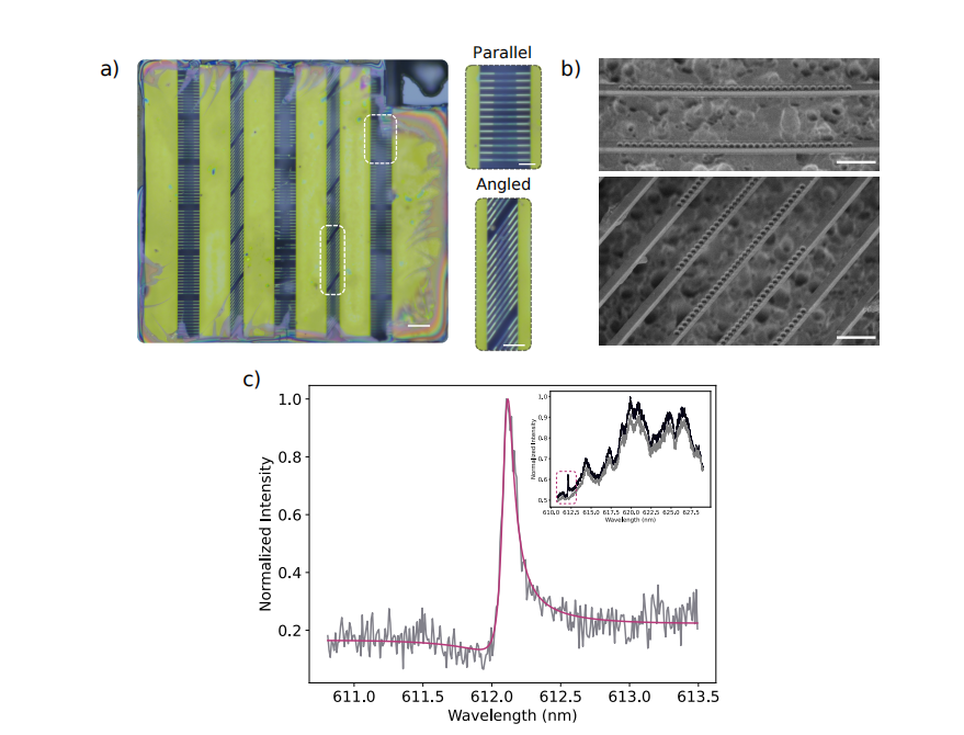
Fabrication of Photonic Crystals: The researchers created 1D photonic crystal cavities in thin-film diamond, achieving high-quality factors (up to 6000) and up to a 12-fold reduction in emitter lifetime. These cavities were designed to enhance the spontaneous emission of SnV− centers, with transitions C and D being studied in detail. The devices were fabricated with specific lattice spacing adjustments to optimize resonance with the SnV− zero-phonon line (ZPL).
Purcell Factor and Lifetime Reduction: Lifetime reduction measurements were used to quantify the Purcell factor, which describes the enhancement in spontaneous emission. The study rigorously analyzed the emission dynamics of both C and D transitions, determining the branching ratio (ηBR) between these transitions to be 0.7815. The maximum Purcell factor observed was 26.21 for the C transition.
Cavity Orientation and Device Characterization: The paper explores the effects of cavity orientation on the Purcell factor, finding that alignment of the cavity mode with the dipole orientation of the SnV− transition is crucial for maximizing emission enhancement. The study also discusses the secondary emitter present in the angled cavity mode, which demonstrated different emission characteristics compared to the primary emitter.
Quantum Network Scalability: These results provide essential steps toward scalable quantum networks based on SnV− centers. The study demonstrates the importance of both efficient photon emission and the precise alignment of photonic cavities with quantum emitters to enhance performance.
In conclusion, the paper presents an important advancement in the field of quantum photonics, highlighting the potential of SnV− centers in thin-film diamond for building efficient quantum network nodes through the enhancement of optical transitions using photonic crystal cavities.
OMeda (Shanghai Omedasemi Co.,Ltd) was founded in 2021 by 3 doctors with more than 10 years of experience in nanpfabrication. It currently has 15 employees and has rich experience in nanofabrication (coating, lithography, etching, two-photon printing, bonding) and other processes. We support nanofabrication of 4/6/8-inch wafers.