This paper discusses the use of chiplet-based technology for the development of scalable trapped-ion quantum processors (TIQCs). The authors propose a modular system where various processor components, or "chiplets," are fabricated separately and then integrated using heterogeneous packaging techniques. This chiplet approach contrasts with traditional monolithic designs, offering flexibility and reducing the complexity and costs associated with scaling up TIQCs.
Key points include:
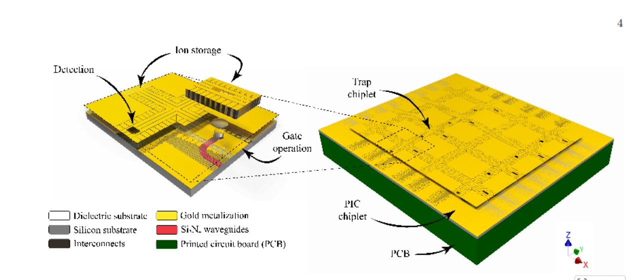
Modular Chiplet Architecture: The chiplet system separates various functionalities into different chiplets. The ion trap is placed on a dielectric substrate, while photonic integrated circuits (PICs) handle optical signal routing and application-specific integrated circuits (ASICs) manage electrical signals. This approach allows for the use of optimal materials and manufacturing technologies for each chiplet, improving overall performance and flexibility.
Technology and Fabrication: The paper details the fabrication of the chiplets, which include a trap chiplet for ion storage, a PIC chiplet for light routing, and an ASIC layer for electrical control. The use of metal-filled through-substrate vias (TSVs) for electrical interconnects and microfabricated optical components (e.g., focusing units) demonstrates the integration of different technologies into one scalable package.
Demonstration of Optical Addressing: The authors demonstrate the potential of this chiplet-based approach through a prototype of an optical addressing system for individual ions in a 10-ion crystal. The system uses microfabricated lenses placed on top of a PIC chiplet to focus laser light onto the ions, achieving diffraction-limited spot sizes for precise ion control.
Advantages over Monolithic Integration: The chiplet approach offers several advantages over traditional monolithic integration, such as the ability to optimize each functional component (ion trap, optics, electronics) individually. It also allows for easier modifications and faster iterations, facilitating the development of new functionalities without needing to redesign the entire system.
Future Directions: The authors suggest further improvements to the optical system and the integration of more advanced technologies, such as microheaters for ion loading, integrated photodetectors for readout, and active photonic components for laser control. Additionally, they foresee the use of this technology for more complex ion-trap architectures, including 3D segmented traps.
In conclusion, the chiplet-based architecture provides a promising path forward for scaling trapped-ion quantum processors, enabling the integration of diverse technologies in a cost-effective and modular fashion, while reducing fabrication complexity.
OMeda (Shanghai Omedasemi Co.,Ltd) was founded in 2021 by 3 doctors with more than 10 years of experience in nanpfabrication. It currently has 15 employees and has rich experience in nanofabrication (coating, lithography, etching, two-photon printing, bonding) and other processes. We support nanofabrication of 4/6/8-inch wafers.