This article presents the fabrication of solid-state nanopores using Extreme Ultraviolet (EUV) lithography, marking the first successful wafer-scale production of nanopores down to approximately 10 nm in diameter within silicon nitride (Si3N4) membranes. This approach integrates EUV lithography and a spacer technique to achieve highly uniform and precisely controlled pores across the wafer.
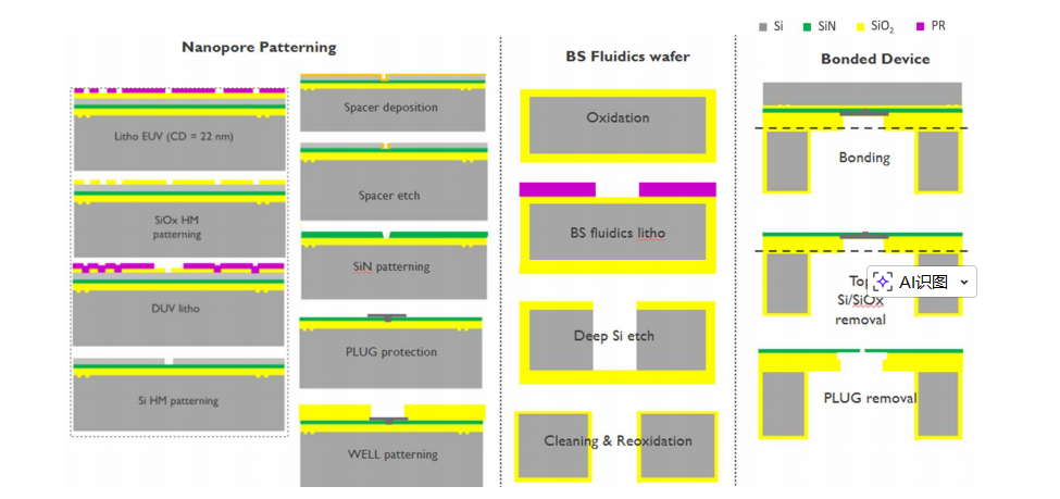
The fabrication process involves two key wafers: a nanopore wafer and a fluidic wafer, which are bonded together to create the nanopore device. The nanopore is fabricated using a dual hard mask technique with amorphous silicon and SiO2 masks, followed by spacer deposition to further reduce the pore diameter. The use of EUV lithography is pivotal in patterning the pores to sub-10 nm dimensions, confirmed by metrology tools such as CD-SEM (Critical Dimension Scanning Electron Microscopy) and Transmission Electron Microscopy (TEM).
Characterization of the nanopores includes electrical measurements in ionic solutions, revealing their ionic current-voltage (I-V) characteristics, resistance, and noise performance. The nanopores were also tested for DNA translocation, showing their effectiveness in molecular sensing, with a high signal-to-noise ratio (SNR). The experiments demonstrated that the nanopores can distinguish different configurations of DNA molecules as they translocate through the pore.
The paper concludes that EUV lithography-based nanopore fabrication shows significant potential for large-scale production of nanopores with tunable dimensions, paving the way for advanced applications in molecular sensing, including DNA analysis and other data storage technologies.
OMeda (Shanghai Omedasemi Co.,Ltd) was founded in 2021 by 3 doctors with more than 10 years of experience in nanpfabrication. It currently has 15 employees and has rich experience in nanofabrication (coating, lithography, etching, two-photon printing, bonding) and other processes. We support nanofabrication of 4/6/8-inch wafers.