This article discusses the development and testing of co-packaged optics (CPO) for high-performance optical interconnects. The focus is on the packaging process and performance characteristics of optical waveguides (PWGs) integrated into silicon substrates.
CPO Packaging Types and Testing: The study presents two types of CPO packaging—Type-A and Type-B—designed for optimal integration with optical and electrical components (as shown in Figure 1). The paper includes detailed tests, such as peel and pull tests, to assess the strength and reliability of the package connections under different environmental conditions (moist and dry).
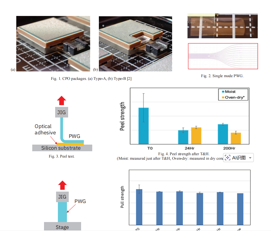
Waveguide and Optical Adhesive: The work highlights the use of single-mode PWGs, demonstrating their performance and reliability in optical communication systems (Figure 2). The peel strength, which reflects the adhesion quality of the optical adhesive used, was measured under various conditions, showing that different treatments (oven-dry vs. moist) can affect the adhesive’s performance (Figure 4).
Thermo-Mechanical Models and Stress Distribution: The paper uses thermo-mechanical modeling to understand the stress distribution within the optical packages. The results, shown in Figures 8-10, indicate how the different materials in the package—such as silicon, laminate, and ferrules—respond to thermal conditions, which is crucial for maintaining device integrity during operation.
Insertion Loss Testing: Insertion loss, a key performance metric for optical systems, was measured before and after reflow processes. The results, displayed in Figure 7, demonstrate the minimal impact of reflow on the insertion loss, indicating good thermal stability and performance after packaging.
Chiplet Package Design: The paper also explores the design of chiplet packages, which are modular systems used to integrate multiple optical interfaces within a single package. Figure 12 presents a schematic of such a chiplet package, showcasing the potential for high-density, scalable optical interconnects.
The overall goal of this research is to enhance the reliability and efficiency of optical interconnects, particularly for high-speed data transmission systems in AI and computing applications. The results point to the successful development of robust CPO packages that can support next-generation optical I/O technologies.
OMeda (Shanghai Omedasemi Co.,Ltd) was founded in 2021 by 3 doctors with more than 10 years of experience in nanpfabrication. It currently has 15 employees and has rich experience in nanofabrication (coating, lithography, etching, two-photon printing, bonding) and other processes. We support nanofabrication of 4/6/8-inch wafers.