This paper discusses the role of silicon photonics in advancing sustainable AI infrastructure, focusing on the integration of photonics with traditional electronics to overcome the energy challenges posed by the rapid growth of AI and data processing demands. It explores innovations in optical interconnects, switches, and neural networks, arguing that the combination of photonic and electronic technologies, optimized holistically, will be key to achieving energy-efficient AI infrastructure.
Energy Efficiency in AI Infrastructure:
As AI workloads grow, they lead to increased energy consumption. To address this, the paper advocates for silicon photonics as a way to decouple data increase from energy increase.
Silicon photonics can provide energy-efficient high-density interconnects, low-energy optical path switching, and enable photonic neural networks (PNNs), which perform computations at the speed of light, making them ideal for accelerating AI.
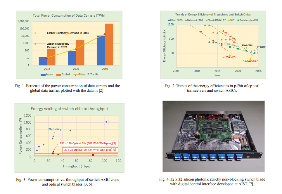
Scaling Challenges with Optical Transceivers and Switches:
The paper compares the energy efficiency of optical transceivers and switch ASICs used in data centers. It shows that while optical transceivers have significantly improved energy efficiency, switch ASICs have not kept pace, resulting in higher power consumption as throughput increases.
Replacing electrical switches with optical switches can reduce network power consumption by up to 75% in composable disaggregated infrastructures.
System Use Cases of Optical Switches:
Optical switches are limited by their inability to process packets like electrical switches (i.e., they function as optical circuit switches, not packet switches). This requires a control plane and an orchestrator to manage the system differently from conventional packet-based systems.
AIST has developed large-scale silicon photonic switches capable of 32 x 32 non-blocking connections and demonstrated their potential for energy efficiency in AI infrastructures. These switches are made using standard CMOS technology and have the scalability to handle thousands of devices.
Photonics for Neural Networks:
Photonic neural networks (PNNs) are explored as a way to accelerate AI computations. These networks perform matrix-vector multiplications (MVM) optically, without consuming energy during computation, unlike traditional digital processors like GPUs.
The challenge is that PNNs currently lack effective nonlinear activation functions for AI tasks. The paper proposes using electro-optic (EO) nonlinearities to address this, enabling nonlinear activation through photonic circuits.
Several AI models using EO nonlinearities are demonstrated, including a nonlinear projection mapping and a cascaded vertical hierarchical EO-PNN model, which shows good accuracy for tasks like MNIST classification.
EO Hopfield Network:
The paper introduces an EO Hopfield network using MZI devices (Mach-Zehnder Interferometers) as nonlinear neurons. This network can store and recall patterns, showcasing its potential for associative memory tasks in AI.
Streaming PNNs:
The paper suggests a streaming PNN model, where photonics are used for matrix-vector multiplications (MVM) in a mixed electrical-optical system. This model allows the PNN to stream-process data in both domains, seamlessly integrating into digital infrastructures.
The paper concludes that silicon photonics holds significant potential to sustain AI infrastructure by offering energy-efficient solutions for high-density interconnects, optical switching, and photonic neural networks. However, for these photonic technologies to be fully integrated into existing systems, a holistic approach to architecture optimization involving both hardware and software is required. The integration of CMOS and photonics will enable scalable, low-energy AI computing, with photonic neural networks playing a crucial role in reducing the energy consumption of future AI systems.
OMeda (Shanghai Omedasemi Co.,Ltd) was founded in 2021 by 3 doctors with more than 10 years of experience in nanpfabrication. It currently has 15 employees and has rich experience in nanofabrication (coating, lithography, etching, two-photon printing, bonding) and other processes. We support nanofabrication of 4/6/8-inch wafers.