The article titled "High-gain optical parametric amplification with a continuous-wave pump using a domain-engineered thin-film lithium niobate waveguide" demonstrates a significant advancement in on-chip optical signal amplification. Here is a summary of the key points:
The article addresses the challenges of optical parametric amplification (OPA) for integrated optical communication circuits. Thin-film lithium niobate (TFLN) is a promising material for integrated photonic devices due to its high efficiency in signal generation. However, on-chip signal amplification has been a challenge. Traditional optical amplifiers, like erbium-doped fiber amplifiers (EDFAs), are used off-chip, but on-chip solutions are needed for more compact devices. This study demonstrates the use of continuous-wave (CW) pumping in TFLN waveguides for high-gain optical parametric amplification.
The researchers utilize a cascaded second-harmonic generation (SHG) and OPA process to achieve high on-chip gain. The SHG process is used to generate the pump light, which is then used for OPA. This indirect-pump geometry simplifies the design and ensures efficient coupling. The resulting high gain is demonstrated over a broad 110 nm bandwidth, covering both the C and L bands of the telecom spectrum. The on-chip parametric gain achieved is as high as 13.9 dB, with the device demonstrating excellent performance for communication signal amplification.
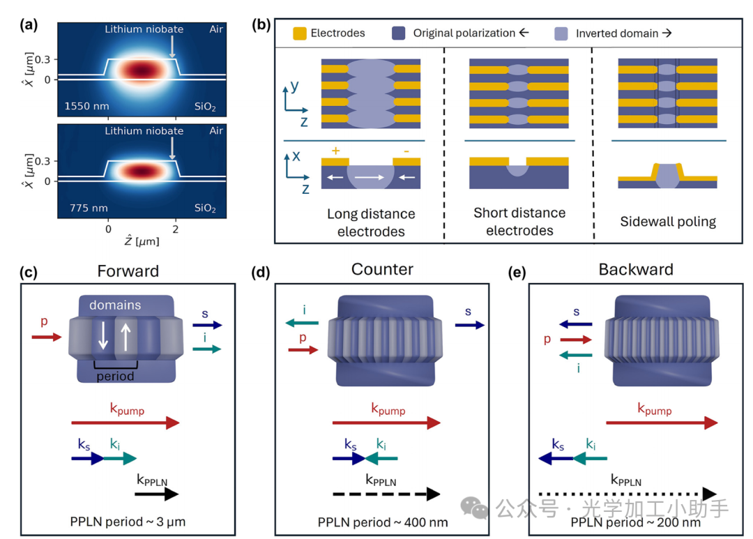
The OPA device is fabricated on an x-cut TFLN wafer using a wafer-scale process that is common for devices such as electro-optic modulators (EOMs). Domain-engineered waveguides are created using deep-ultraviolet (DUV) lithography. A focused ion-beam trimming technique is employed to reduce film thickness variations across the wafer, which is crucial for achieving high nonlinear efficiency. The fabrication also eliminates selective etching problems typically encountered in domain-engineered TFLN waveguides.
SHG Efficiency: The SHG power measurement across different chips shows that the device from the central part of the wafer (chip #10) exhibits peak efficiencies of up to 2670%/W.
OPA Performance: In the OPA experiment, the signal power is significantly amplified, with an on-chip gain of 13.9 dB and a net gain of 9.9 dB, after accounting for device insertion losses.
Signal-to-Noise Ratio (SNR): The amplified signal shows a lower bit error rate (BER) compared to the case without amplification, especially for lower signal powers. The OPA device achieves an excellent optical signal-to-noise ratio (OSNR) consistently above 28 dB across various bandwidth settings.
The OPA device is tested for modulated signal amplification using commercial optical communication modules with data rates of 1.25 and 3.125 Gbps. The experimental setup confirms that with OPA, the signal power as low as −44 dBm can be amplified to a detectable level. The BER is significantly reduced compared to the unamplified signal. The performance of the OPA device is found to be better than that of traditional EDFAs at the same power levels.
This work demonstrates a high-gain optical parametric amplifier (OPA) with a CW pump using TFLN waveguides. The device shows a broad gain bandwidth, high fidelity, and low noise, making it a promising candidate for integrated optical communication systems. The device is fabricated using a wafer-scale process, compatible with other TFLN devices like electro-optic modulators, paving the way for fully integrated optical communication circuits. The results show that the OPA device could be further optimized for power efficiency and integrated with other TFLN devices for more compact and efficient systems.
Future improvements could focus on reducing the power consumption of the OPA device and increasing the on-chip gain by optimizing the waveguide dimensions and addressing issues related to thickness variations across the TFLN wafer. Additionally, hybrid integration with other photonic components like modulators could further enhance the functionality of the OPA device in integrated communication circuits.
OMeda (Shanghai Omedasemi Co.,Ltd) was founded in 2021 by 3 doctors with more than 10 years of experience in nanpfabrication. It currently has 15 employees and has rich experience in nanofabrication (coating, lithography, etching, two-photon printing, bonding) and other processes. We support nanofabrication of 4/6/8-inch wafers.