The article titled "Long optical and electron spin coherence times for erbium ions in silicon" investigates the properties of Er³⁺ ions embedded in silicon, specifically focusing on their optical and electron spin coherence times, which are key for quantum information processing (QIP). Here is a summary of the main points:
Erbium (Er³⁺) ions are promising candidates for quantum information applications due to their telecom-compatible optical transitions and spin coherence properties. Silicon, being a highly compatible platform for quantum technologies, offers significant advantages for QIP, including mature fabrication methods and scalability. The study aims to assess Er³⁺ ions in silicon, which have potential for use in spin-photon interfaces crucial for quantum computing and networks.
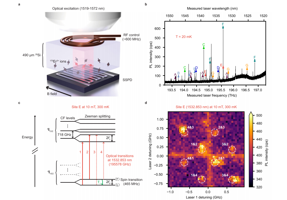
Long Coherence Times: The study reports exceptionally long electron spin coherence times of 0.8 ms and 1.2 ms for Er³⁺ ions in silicon at two different sites (Site E and Site F). These values are significant compared to previous studies on Er³⁺ ions in silicon, where spin coherence times were much shorter due to interference from nuclear spins in natural silicon.
Optical Properties: The Er³⁺ ions exhibit narrow inhomogeneous linewidths (around 148 MHz and 72 MHz for Site E and Site F, respectively), which are key for achieving high cooperativity in spin-photon interactions. The homogeneous linewidths are even narrower, with values below 70 kHz, indicating high optical coherence and making these sites suitable for use in high-fidelity quantum applications.
Spectral Hole Burning: To determine the homogeneous linewidths, the researchers used a spectral hole-burning technique. The measurements reveal that the homogeneous linewidths of the Er³⁺ sites in silicon are among the narrowest observed for this material, which is important for applications requiring stable and coherent photon emissions.
Spin-Transition Measurements: Optically detected magnetic resonance (ODMR) was used to study the spin transitions. The observed Rabi frequencies for spin flips are high, exceeding 1.7 MHz, which suggests fast spin manipulation is possible. The Hahn echo decay measurements further confirm long spin coherence times, and the measurements show that external noise sources, such as mechanical vibrations, may contribute to small variations in the observed coherence times.
Quantum Information Processing (QIP): The long optical and spin coherence times of the Er³⁺ ions in silicon make them excellent candidates for use in quantum information processing. They can be employed in spin-photon interfaces, which are essential for creating scalable quantum networks and computers.
Enhanced Fabrication: The study highlights the potential of using silicon for large-scale integration of Er³⁺-based quantum devices. Silicon photonic crystals with high quality factors can further enhance the performance of Er³⁺ ions embedded in silicon by improving the coupling between the ions and nanophotonic cavities.
Improved Performance: While the results are promising, future research could focus on improving the spin coherence times even further by minimizing external noise sources and optimizing the implantation and annealing processes for better uniformity and performance. Additionally, further studies on single Er³⁺ ion measurements and their integration with other quantum systems could lead to the development of more robust and scalable quantum technologies.
This study marks a significant step forward in the development of Er³⁺ ions in silicon as a platform for quantum information processing. The long coherence times observed in both optical and spin transitions, combined with the silicon-based technology's scalability, position Er³⁺:Si as a promising candidate for future quantum networks and computation applications.
OMeda (Shanghai Omedasemi Co.,Ltd) was founded in 2021 by 3 doctors with more than 10 years of experience in nanpfabrication. It currently has 15 employees and has rich experience in nanofabrication (coating, lithography, etching, two-photon printing, bonding) and other processes. We support nanofabrication of 4/6/8-inch wafers.