This paper explores erbium (Er)-implanted silicon (Si) as a platform for quantum technologies (QTs), particularly for quantum communication and quantum computing. Erbium, a rare-earth (RE) ion, is appealing due to its compatibility with telecommunications wavelengths (around 1.5 µm), long coherence times, and integration with established silicon fabrication techniques used in the semiconductor industry.
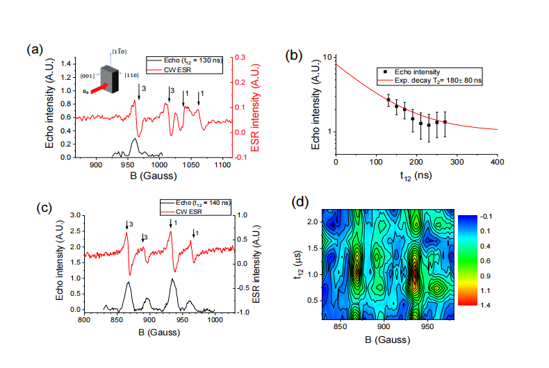
The study reports the first coherence measurements of Er in Si, showing a spin coherence time (T2) of approximately 10 µs at 5 K for an Er concentration of 3×10¹⁷ cm⁻³. The Er ions are found to be coupled with oxygen (O) atoms, forming an Er-O defect complex. This interaction results in a previously unreported energy state, which facilitates non-radiative relaxation and could make optical spin polarization of the Zeeman ground state feasible, similar to the NV center in diamond.
In addition, the paper demonstrates strong coupling between Er-implanted Si and a superconducting (SC) resonator, with coupling strength around 1 MHz. This is a significant step toward hybrid quantum circuits, which combine the long coherence times of silicon-based qubits with the faster processing capabilities of superconducting qubits. Such systems could enable quantum information processing over telecommunications networks.
The results also show that Er implanted Si can function as a viable quantum communication platform, with potential for high-temperature operation and scalability. The findings suggest that Er-implanted Si could bridge the gap between solid-state quantum computing and quantum communication, offering a promising path for future hybrid quantum devices.
OMeda (Shanghai Omedasemi Co.,Ltd) was founded in 2021 by 3 doctors with more than 10 years of experience in nanpfabrication. It currently has 15 employees and has rich experience in nanofabrication (coating, lithography, etching, two-photon printing, bonding) and other processes. We support nanofabrication of 4/6/8-inch wafers.