This paper explores the integration of Erbium (Er³⁺) emitters into silicon-on-insulator (SOI) metasurfaces, aiming to enhance the collection efficiency of Er³⁺ emission at telecom wavelengths, particularly around 1535 nm. The SOI metasurfaces were fabricated using silicon nanodisks, which were designed to improve the spontaneous emission properties of Er³⁺ ions embedded in the silicon layer, making the system CMOS-compatible and scalable for future quantum technologies.
The study demonstrates a significant enhancement in photoluminescence (PL) from Er³⁺ ions embedded in the metasurfaces, with a maximum experimental enhancement factor of 5 observed at room temperature. The authors show that the fabrication of SOI metasurfaces with Er-implanted nanodisks can effectively increase the photon extraction efficiency, while also improving the emission characteristics at both room and cryogenic temperatures.
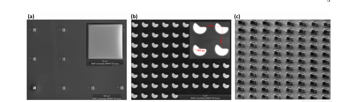
Key findings include the observation of stronger PL signals and reduced optical lifetime in the metasurfaces compared to unpatterned SOI regions. Time-resolved spectroscopy reveals that the optical lifetime is reduced by approximately 9.6% due to the metasurface design, and polarization measurements suggest that the metasurfaces enhance the alignment of the emission dipole with the crystal axis.
Additionally, the paper presents photoluminescence excitation (PLE) spectroscopy, which identifies distinct Er³⁺ transitions and shows that the metasurfaces enhance emission at specific wavelengths. The results indicate that these SOI metasurfaces, by tuning the nanostructure design, can be used to control and improve the properties of Er³⁺ emitters, making them suitable for applications in quantum photonics and integrated telecom light sources.
In conclusion, the work shows that SOI metasurfaces can enhance Er³⁺ emission, offering a promising platform for integrating rare-earth emitters into scalable, CMOS-compatible quantum technologies. Future work aims to optimize the metasurface design for further enhancement of the emission rate and lifetime properties.
OMeda (Shanghai Omedasemi Co.,Ltd) was founded in 2021 by 3 doctors with more than 10 years of experience in nanpfabrication. It currently has 15 employees and has rich experience in nanofabrication (coating, lithography, etching, two-photon printing, bonding) and other processes. We support nanofabrication of 4/6/8-inch wafers.