Shanghai Aomeda Micro provides silicon carbide photolithography and etching processing, targeting the current market for:
Silicon carbide power devices
Silicon carbide diffraction optical waveguides
Silicon carbide photonic integrated circuits
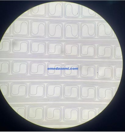
Silicon carbide microfluidic channels
Shallow etching of silicon carbide with small linewidth.
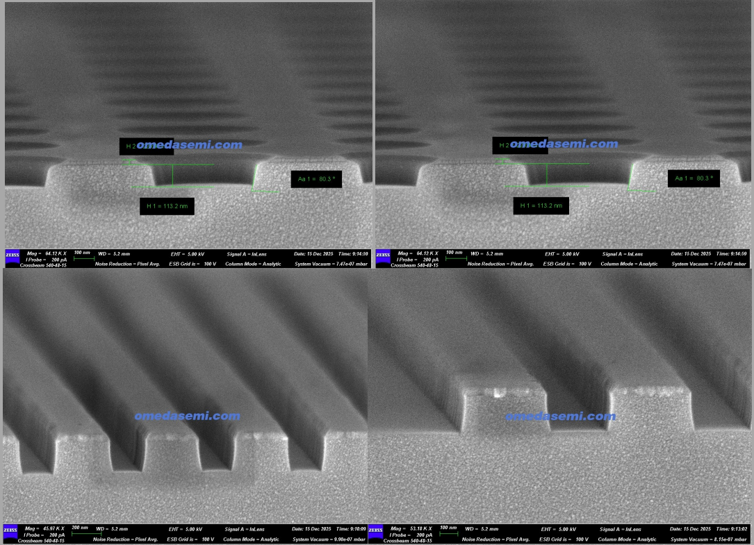
Currently, the demand for silicon carbide in optical applications primarily involves etching at the nanometer scale. By combining DUV and electron beam lithography and etching processes, we can perform silicon carbide etching with small linewidths.
The minimum linewidth is 150nm, with an etching aspect ratio of 5:1.
Deep etching of silicon carbide with large linewidth.
Etching process parameters:
Etching methods: Reactive Ion Etching (RIE), Deep Reactive Ion Etching (DRIE), Inductively Coupled Plasma Etching (ICP)
• Maximum etching depth: >150 μm
• Etching rate:
• Large linewidth (>200 μm): >2 μm/min
• Small linewidth (50-100 μm): 0.5-1.5 μm/min
• Etching uniformity: ±5% (within a 100 mm diameter range)
• Sidewall angle: 89°-91°
Selectivity: SiC/mask layer (SiO₂, PR, etc.) > 10:1
• Roughness: <10 nm (sidewalls)
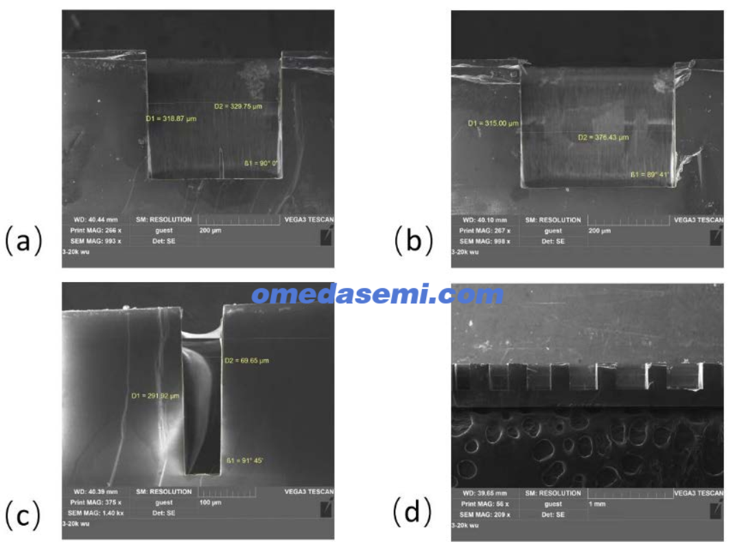
2.2 SEM Analysis
Based on SEM images (shown below), we summarize the etching capabilities as follows:
• (a)-(b) Large linewidth etching (350 μm, 400 μm)
• Sidewall angle close to 90°, uniform etching depth.
• Faster etching rate, good surface morphology.
• (c) Small linewidth etching (75 μm)
• Etching depth is lower compared to large linewidth etching.
• Sidewalls still maintain good verticality, but etching rate decreases.
• (d) Array structure etching (250-500 μm)
• Improved morphology, verticality, and etching profile.
• Suitable for sensor, microfluidic, and other micro/nano structure fabrication.