website:en.omedasemi.com
email:jing.chen@omeda-optics.com
Background
Recently, many scientists take efforts on the development of periodically polarized thin-film lithium niobate devices and thin-film lithium tantalate devices.
''The dispersion and QPM condition are sensitive to TFLN waveguide dimensions in cross-section. Specifically, the current TFLN wafers are normally fabricated with total thickness variation (TTV) on the order of tens-of-nanometers, and thus dramatically change the phase matching and reduce the parametric gain [42]. This makes it difficult to achieve high overall nonlinear efficiency (PSHG/P2FW, PSHG: SHG power, and PFW: FW power) from domain-engineered TFLN waveguides。''
Therefore,Ultra uniform and low roughness is very important for periodically polarized thin-film lithium niobate devices and thin-film lithium tantalate devices.
Current Situation:
NOTE:
before the following information ,i want to declare some parameter of LNOI wafer
LN thickness Variation or Range :test a few points'thickness of LN thin film,and Variation/range=the biggest data-the smallest data
LN thickness Mean/Average:test a few points'thickness of LN thin film,and calculate the mean data of these points .
TTV BOW Wrap is data relate to total wafer not LN film
The standard 6-inch LNOi LNThickness Variation sold on the market is 140A-160A, and the roughness is 0.15nm-0.18nm.
For electro optical modulator device ,it is fine ,but for PPLN or PPLT device ,it is not so good .
Our Innovation(For Ultra Uniform LN/LT Layer ):
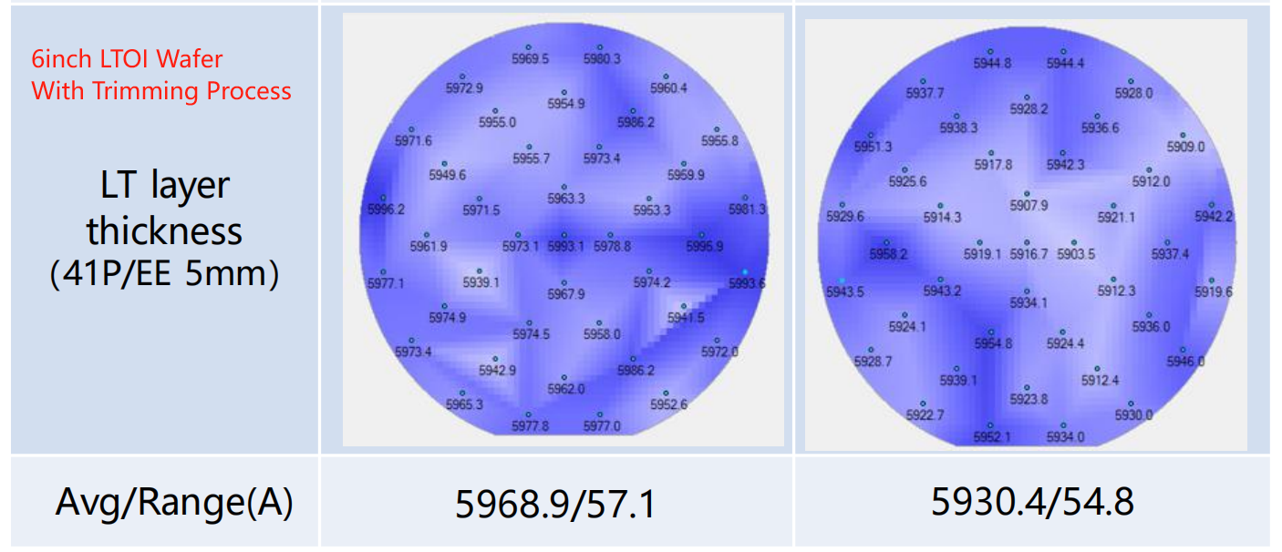
Compared with general LNOI wafer ,we add a innovative process:"Gas Cluster Ion Beam Trimming process " to improve the uniformity(Thickness uniformity From 140A-160A to Range<57A) of LN thickness .
For Example:
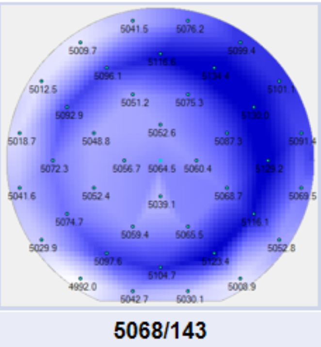
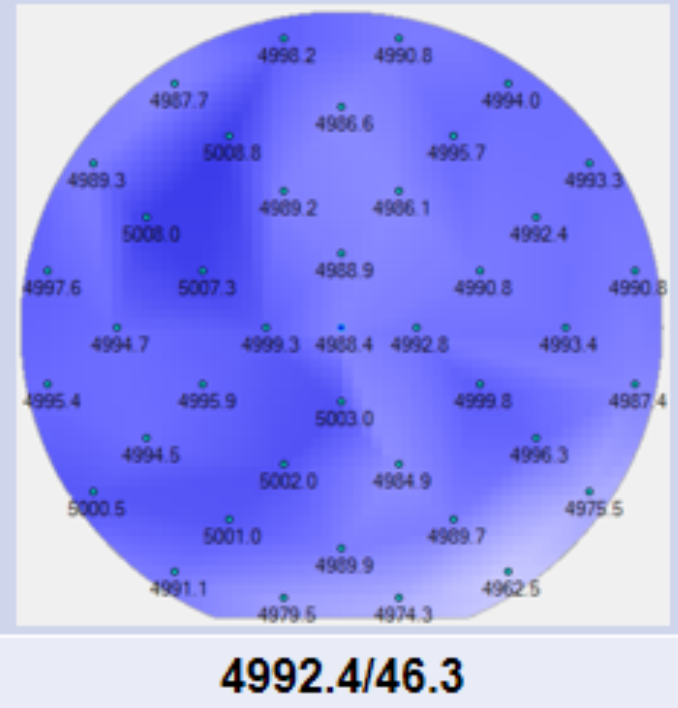
As you can see of the following 2 pictures ,the more uniform wafer show more uniform color
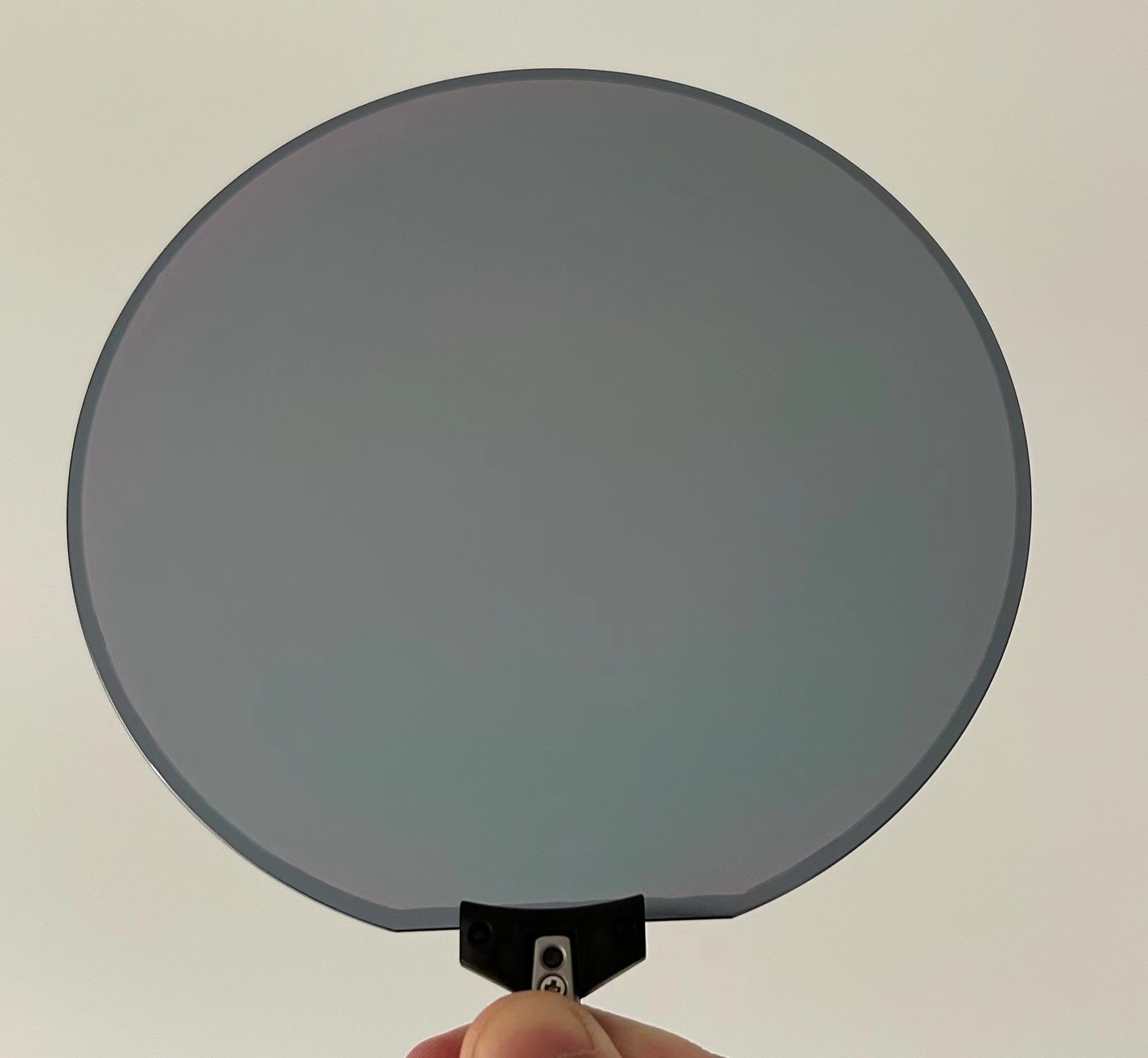
6 inch MgO Doped LNOI Wafer Without Trimming Service: Range 143A
6 inch LTOI Wafer Without Trimming Service: Range 100A-200A
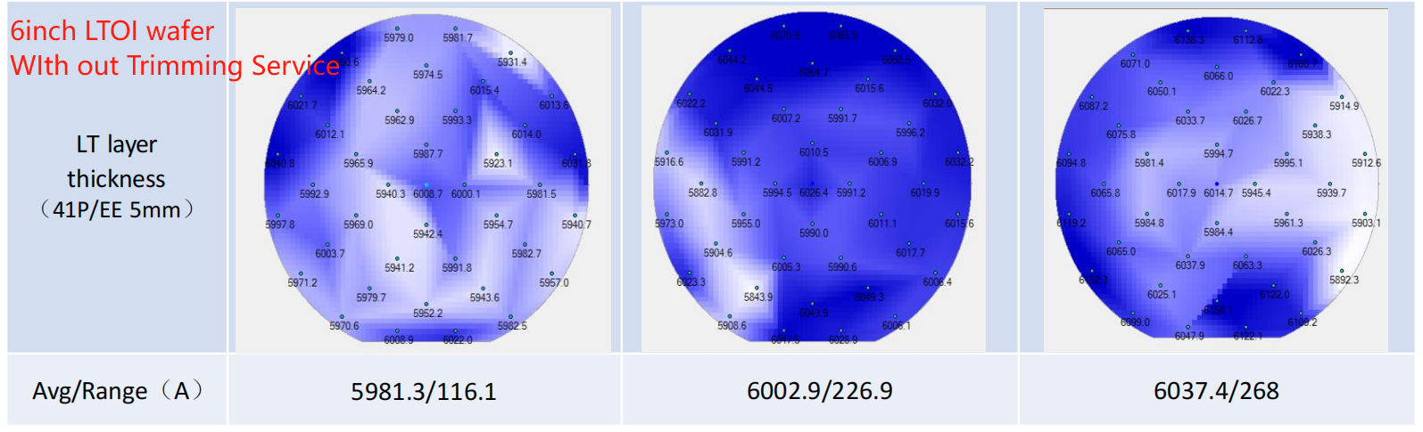
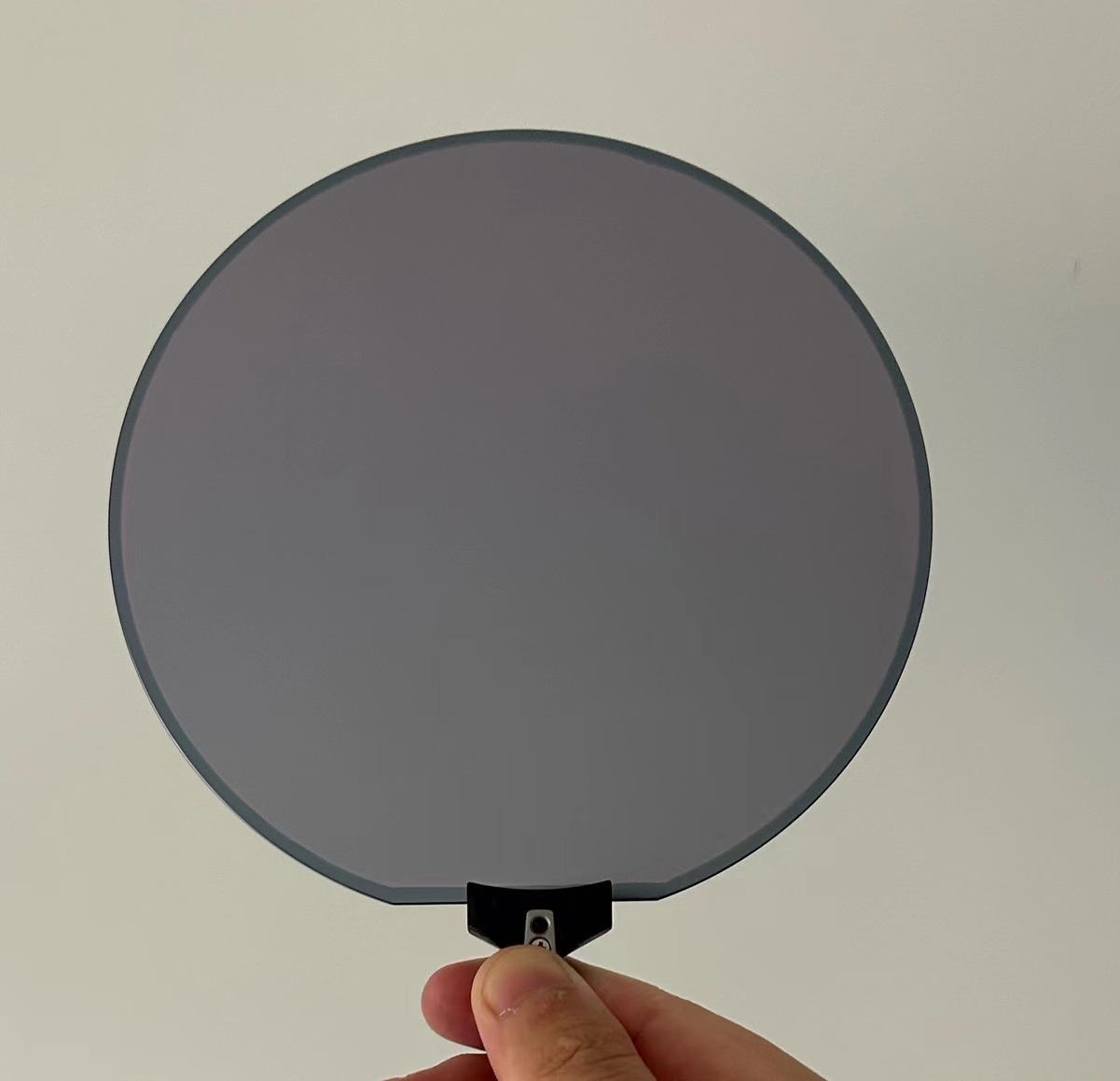
6 inch LTOI Wafer With Trimming Process:Rangelithium tantalate on insulatorlithium tantalate on insulator without trimming:<57A
Compared with RIE or IBE Trimming Machine:(Please click to know more about the " Gas Cluster Ion Beam Trimming Process")
omeda Trimming have smaller beam size(GCIB:4-5mm,others:10mm) ,and can cntrol smaller area 'uniformity
omeda Trimming cause less damage to crystal and release less heat in chamber to get the best crystal quality.
OMeda (Shanghai Omedasemi Co.,Ltd) was founded in 2021 by 3 doctors with more than 10 years of experience in nanpfabrication. It currently has 15 employees and has rich experience in nanofabrication (coating, lithography, etching, two-photon printing, bonding) and other processes. We support nanofabrication of 4/6/8-inch wafers.