Cavity SOI Wafer for MEMS(Grinding +CMP+Ultra uniform Polishing Process)
the Cavity wafer is a product integrating nanofabrication(Litho DRIE Bonding) process and Ultra Precise polishing and grinding process
Our company can provide CavitySOI wafers. To ensure the quality of the top device layer, we maintain a maximum cavity-to-device layer thickness ratio of 45:1. Furthermore, our advantage lies in our ability to produce ultra-high-precision cavities. The smallest line width achieved by other leading CavitySOI companies is 2µm, achieved using contact lithography machines. Our company uses stepper lithography to create handle wafer patterns. Combined with etching processes, we can produce cavities with minimum line widths of 180nm .
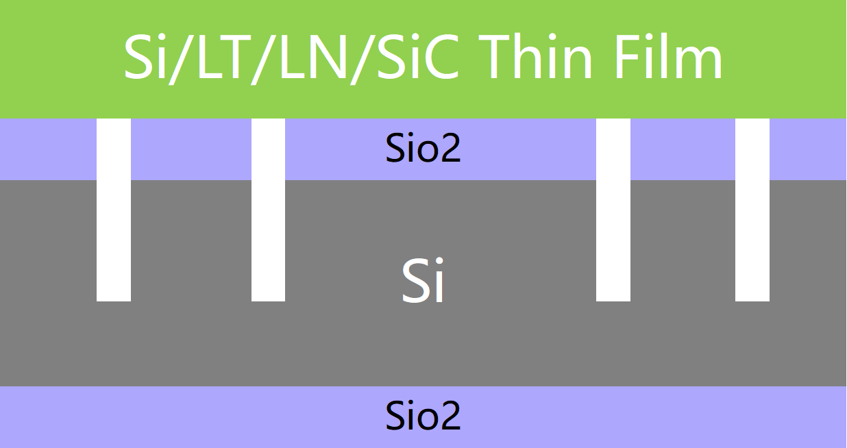
Also we extend the material from silicon to lithium niobate ,lithium tantalate and silicon carbide
Ultra uniform Polishing Process
we use gas cluster ion beam polishing process to trim the device layer and to get the ultra uniform device layer
Normal Cavity SOI Wafer Device Variation:+-1um
Ultra uniform SOI Wafer Device Variation:+-100nm
OMeda (Shanghai Omedasemi Co.,Ltd) was founded in 2021 by 3 doctors with more than 10 years of experience in nanpfabrication. It currently has 15 employees and has rich experience in nanofabrication (coating, lithography, etching, two-photon printing, bonding) and other processes. We support nanofabrication of 4/6/8-inch wafers.