111 Oriented SOI Wafers for GaN Epitaxy in Power Devices - GaN-SOI
Our company has successfully developed 111-orientated SOI wafers for RF GaN epitaxy.
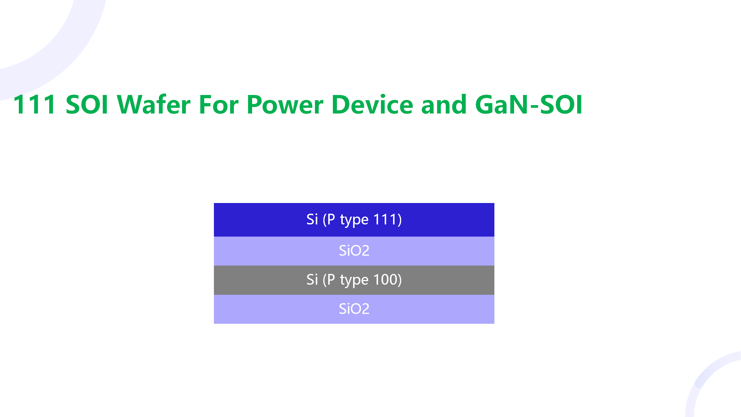
Advantages of Using 111-Oriented SOI Substrates for GaN Epitaxy in Power GaN Devices
"Integrating multiple GaN power devices onto a single chip significantly reduces the size of the power loop, eliminates interconnect parasitics, and reduces assembly complexity. In lateral GaN-on-Si processes, placing multiple power devices on a single chip is straightforward. However, when GaN devices operate at high source-to-substrate voltages, back-gating and threshold voltage shifts can lead to uneven current distribution, reducing efficiency. To fully isolate devices on the same substrate, GaN-on-SOI technology is essential to eliminate back-gating effects and reduce parasitic capacitance."
"Power devices in GaN-on-Si" Monolithic integration on a substrate is hampered by crosstalk between devices and the "backgating" effect caused by substrate contacts. One solution to suppress crosstalk and backgating is to use SOI (silicon-on-insulator) substrates combined with trench isolation. GaN-on-Si devices exhibit a "backganting" effect, in which the silicon substrate affects the electrical characteristics of the channel in the GaN-on-Si structure. This effect can lead to instabilities in threshold voltage and leakage current, thus affecting device performance and reliability. Another solution is to use an engineered substrate with a polysilicon AlN core, commercially available as QST® (QROMIS Substrate Technology). The relatively high price of QST® substrates has hindered their widespread adoption. Recently, there has been significant interest in GaN-on-Sapphire, which can also be used as a substrate for GaN monolithic integrated circuits. A drawback of GaN-on-Sapphire is the low thermal conductivity of sapphire substrates. Therefore, SOI substrates offer a good trade-off between low cost and high performance for monolithic circuits.
OMeda (Shanghai Omedasemi Co.,Ltd) was founded in 2021 by 3 doctors with more than 10 years of experience in nanpfabrication. It currently has 15 employees and has rich experience in nanofabrication (coating, lithography, etching, two-photon printing, bonding) and other processes. We support nanofabrication of 4/6/8-inch wafers.