This paper presents a method for achieving wide bandwidth in an air-coupled piezoelectric micromachined ultrasonic transducer (PMUT) through DC bias tuning. The study focuses on a PMUT made of lead zirconate titanate (PZT) and demonstrates experimental results showing significant improvements in displacement sensitivity and bandwidth.
Key Points:
Wide Bandwidth and High Sensitivity: The PMUT achieved a high displacement sensitivity of up to 5500 nm/V and a 3 dB bandwidth of 20.3 kHz. The wideband performance allows for short pulse transmission, which is crucial for high axial resolution in pulse-echo imaging.
DC Bias Tuning: The DC bias voltage applied to the PZT layer tunes the frequencies of two closely spaced resonance modes in the PMUT. A bias of around ±5V results in the overlap of these modes, leading to a wider bandwidth and shorter pulse transmission.
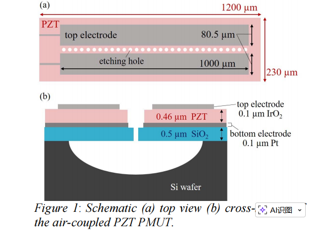
Design and Fabrication: The device uses a ribbon-shaped PMUT, with a rectangular membrane designed to reduce the frequency difference between adjacent working modes. The fabrication involves deposition of PZT and electrode layers, followed by patterning, sacrificial etching, and release processes using XeF2.
Experimental Results: The PMUT showed two vibration modes with frequencies near 175 kHz. With DC bias tuning, the bandwidth increased by a factor of 8.5, and displacement sensitivity improved by a factor of 5. These improvements enable the PMUT to transmit shorter pulses for pulse-echo measurements.
Time Response and Application: The pulse transmission time was reduced from 0.28 ms (without DC bias) to 0.05 ms (with +5V DC bias), enhancing the minimum range for pulse-echo measurements from 19 cm to 3.4 cm.
Conclusion: The DC bias tuning method significantly enhances the performance of air-coupled PMUTs, making them suitable for high-resolution imaging applications without the need for complex resonant tube structures. This approach can be applied to improve PMUT-based systems in various fields like range-finding, imaging, and sensing.
OMeda (Shanghai Omedasemi Co.,Ltd) was founded in 2021 by 3 doctors with more than 10 years of experience in nanpfabrication. It currently has 15 employees and has rich experience in nanofabrication (coating, lithography, etching, two-photon printing, bonding) and other processes. We support nanofabrication of 4/6/8-inch wafers.