This article provides an overview of the recent advancements in hybrid diamond photonics for quantum information processing and sensing. It focuses on the integration of nitrogen-vacancy (NV) centers and other color centers in diamond with cutting-edge photonic platforms, aiming to build scalable systems for quantum applications.
Key points include:
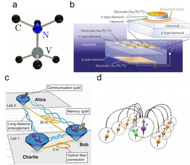
Diamond Quantum Technologies: The paper highlights the significant potential of diamond-based quantum technologies, especially through NV centers, for quantum sensing (e.g., magnetic field, temperature, strain) and quantum information processing (e.g., single-photon sources, quantum memories, and networks). NV centers offer long spin coherence times at room temperature, making them ideal for various quantum applications.
Hybrid Integration: To unlock the full potential of diamond quantum technologies, the hybrid integration of diamond nanostructures with existing photonic platforms such as silicon (Si), silicon nitride (SiN), and lithium niobate (LiNbO₃) is emphasized. This approach offers the ability to combine the best properties of both materials and supports the development of scalable quantum systems.
Nanofabrication Techniques: The article discusses several nanofabrication techniques for creating and integrating color centers in diamond, such as ion implantation, electron irradiation, and laser writing. These methods allow for precise control of defect positions within diamond, which is crucial for high-quality quantum devices.
Challenges and Opportunities: Despite significant progress, challenges remain in terms of scalability, integration with other photonic technologies, and improving the yield and efficiency of quantum sensors. Overcoming these issues requires advances in fabrication techniques, hybrid integration strategies, and new approaches like the "smart cut" technique for creating high-quality diamond membranes.
Quantum Sensing Applications: Diamond-based quantum sensors, particularly those using NV centers, have demonstrated exceptional sensitivity for applications like magnetometry and imaging at the nanoscale. The integration of these sensors into compact, practical devices is an ongoing effort to enable widespread use in fields such as biomedicine and material science.
Future Directions: The paper concludes by exploring the future of diamond quantum photonics, with an emphasis on hybrid integration, improving coherence times, and developing new functionalities for practical quantum sensors and information systems. The goal is to create fully integrated, scalable quantum devices with high performance for a wide range of applications.
This review serves as a comprehensive guide to the current state of hybrid diamond quantum photonics and the significant steps toward realizing practical quantum technologies.
OMeda (Shanghai Omedasemi Co.,Ltd) was founded in 2021 by 3 doctors with more than 10 years of experience in nanpfabrication. It currently has 15 employees and has rich experience in nanofabrication (coating, lithography, etching, two-photon printing, bonding) and other processes. We support nanofabrication of 4/6/8-inch wafers.