This paper presents a scalable fabrication technique for quantum devices based on thin-film diamond, which integrates silicon-vacancy (SiV) quantum memories with photonic crystal cavities. The key innovation is a high-yield, wafer-scale process for the deposition of diamond membranes, combined with precise color center implantation and photonic device fabrication. These devices exhibit strong cooperativity for spin-photon interactions, with the ability to create high-quality quantum memories that can be integrated with silicon-based electronic components.
Key points include:
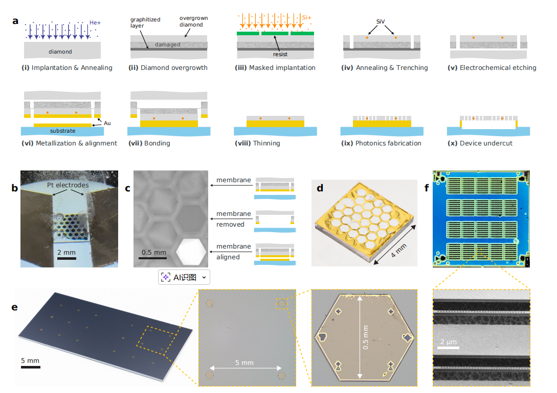
Scalable Fabrication of Diamond Quantum Devices: The authors describe a fabrication pipeline that enables the creation of large-scale arrays of diamond quantum devices with near-unity yield. This includes ion implantation, overgrowth of high-purity diamond films, and bonding to semiconductor substrates. These processes are essential for producing large arrays of SiV-based quantum memories.
High-Cooperativity Spin-Photon Interfaces: The platform supports the creation of photonic crystal cavities that are tightly coupled to SiV centers in diamond. This leads to high cooperativity (C ~ 92), which is crucial for efficient spin-photon interactions. These interfaces are demonstrated to be robust against spectral diffusion, making them suitable for quantum network applications.
Membrane Bonding and Photonic Integration: A key aspect of the fabrication process is the flip-chip thermocompression bonding technique, which allows for the reliable transfer of diamond membranes onto handling chips. This method facilitates the parallel fabrication of many devices on a single chip, paving the way for large-scale production.
Microwave and Optical Integration: The platform is compatible with microwave control, demonstrated using buried coplanar waveguides (bCPWs) for controlling the spin states of implanted NV centers. Efficient optical packaging, with coupling efficiencies greater than 85%, is also achieved, ensuring seamless integration with photonic devices.
Future Directions: The authors suggest that their platform can be further developed to integrate additional photonic and electronic components, enabling the creation of complex quantum devices for scalable quantum networks. They also explore the potential for oxide bonding as a metal-free approach to simplify downstream processing.
In conclusion, the paper presents significant advances in the scalable fabrication of diamond-based quantum memories and sensors. This work provides a foundation for the mass production of quantum devices, which are essential for the realization of large-scale, modular quantum networks and sensors.
OMeda (Shanghai Omedasemi Co.,Ltd) was founded in 2021 by 3 doctors with more than 10 years of experience in nanpfabrication. It currently has 15 employees and has rich experience in nanofabrication (coating, lithography, etching, two-photon printing, bonding) and other processes. We support nanofabrication of 4/6/8-inch wafers.