This article presents a novel design for programmable photonic integrated circuits (PICs) that enable parallel multi-wavelength operations with embedded feedback loops. The key innovation lies in using resonators and tunable active phase layers in a compact architecture to perform universal linear unitary transformations. The feedback loops reduce the need for multiple active layers and allow for multi-frequency operation, which minimizes optical port requirements and power losses.
Key points from the article include:
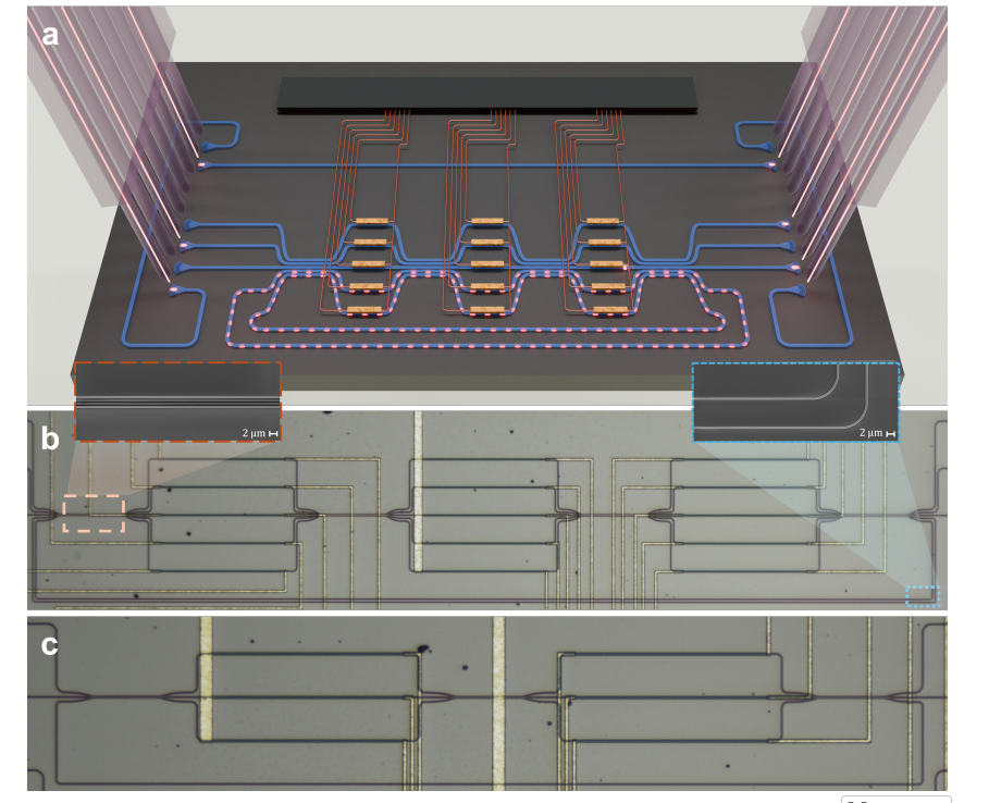
Compact and Scalable Design: The proposed PIC design integrates feedback loops that enable efficient wave mixing and phase control while reducing the number of required layers. This leads to a more compact architecture that can perform multiple operations simultaneously, improving scalability and energy efficiency.
Multi-Frequency Operation: The device can operate in both single and dual-frequency modes, demonstrating the ability to process multiple wavelengths simultaneously. The feedback loops create resonances that narrow the free spectral range (FSR), enabling parallel computing operations across different frequencies.
Experimental Validation: The article describes the fabrication of these circuits on a silicon-on-insulator platform, which is compatible with open-access silicon foundries. The fabricated samples are used to demonstrate the effectiveness of the design in performing linear transformations with high accuracy and low power consumption.
Training and Optimization: The PICs are trained using in situ optimization methods, such as the ADAM optimizer, to achieve desired unitary transformations. The results show that the device can accurately implement several unitary targets, including identity matrices, sparse matrices, and random unitaries, under different operational conditions.
Parallel Computing: The design enables parallel operations by encoding information in different wavelengths. The ability to perform multi-frequency operations is demonstrated, with the system capable of performing matrix-vector multiplications and other linear operations across multiple wavelengths simultaneously.
Theoretical Model and Performance: The theoretical models used to predict the device's behavior are validated experimentally. The model accounts for the transmission matrix and the effects of resonances in the feedback loops, showing that the design can achieve efficient linear transformations with fewer active components than previous methods.
In conclusion, this work introduces a highly efficient and scalable photonic circuit design that leverages feedback loops and multi-wavelength operation for parallel computing. The demonstrated capabilities of these circuits hold promise for future applications in optical computing, quantum information processing, and other areas where fast, energy-efficient computations are required.
OMeda (Shanghai Omedasemi Co.,Ltd) was founded in 2021 by 3 doctors with more than 10 years of experience in nanpfabrication. It currently has 15 employees and has rich experience in nanofabrication (coating, lithography, etching, two-photon printing, bonding) and other processes. We support nanofabrication of 4/6/8-inch wafers.