This chapter outlines the state-of-the-art micro- and nanofabrication techniques for creating photonic devices using single crystal diamond (SCD). It covers various preparation, patterning, and etching processes necessary for structuring diamond at the micro- and nanoscale to support quantum technologies and photonics applications.
Key points from the chapter include:
Substrate Preparation: SCD substrates require substantial preparation due to their natural polycrystalline rim and non-flat surface. Methods such as laser cutting, grinding, and polishing are essential to smoothen and planarize the substrates. Laser cutting is used for initial shaping, followed by grinding and polishing to reduce surface roughness. Mechanical polishing (MP) is typically employed, although it can leave microcracking and roughness that needs to be addressed with additional processes such as thermochemical polishing or reactive ion etching (RIE).
Cleaning and Surface Engineering: Diamond surfaces need to be cleaned to remove particles and contaminants from the polishing process. Typical cleaning methods involve ultrasonic baths, acid cleaning (e.g., piranha solution), and occasionally oxygen plasma cleaning. These processes ensure a clean surface suitable for subsequent patterning and etching. Surface termination is important for adhesion of subsequent layers and the behavior of color centers.
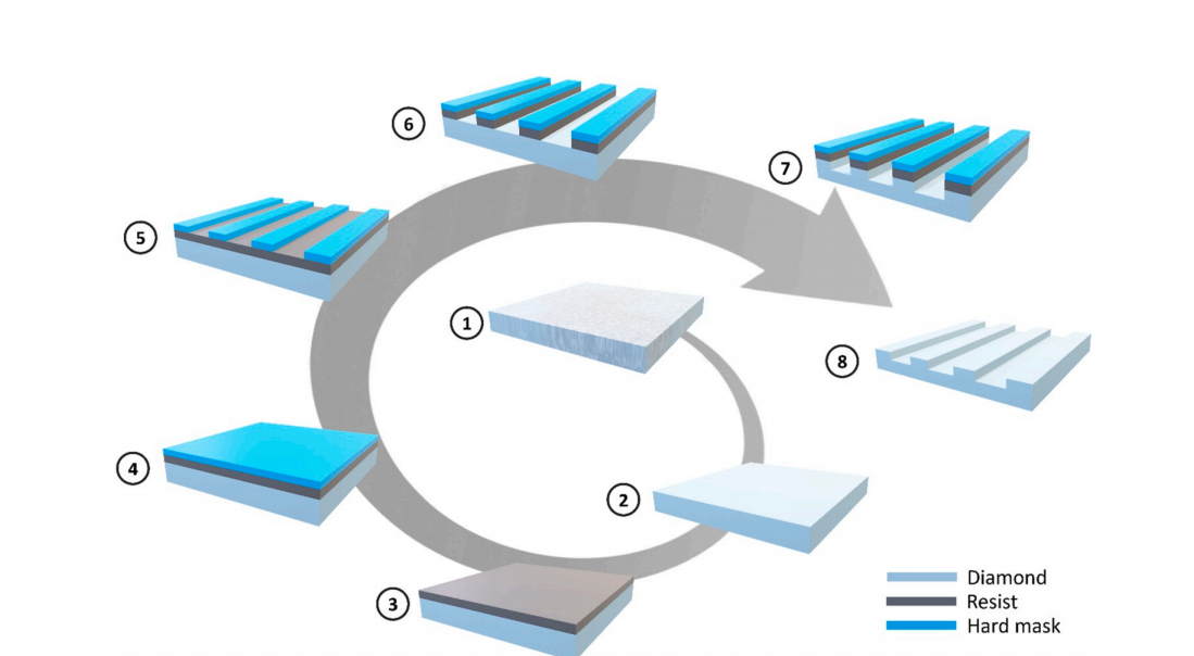
Patterning Techniques: Patterning SCD involves using lithography methods such as photolithography and electron-beam lithography. These techniques are essential for transferring designs onto the diamond substrate. Photolithography is useful for larger-scale patterns, while electron-beam lithography is ideal for high-resolution micro- and nanostructures. Direct patterning methods, such as focused ion beam (FIB) milling and electron-beam-induced etching (EBIE), are also discussed. FIB offers flexibility but induces ion damage, which can affect the material’s properties, especially in applications like quantum sensing.
Etching Techniques: The chapter discusses different etching methods, including high-temperature etching, catalyst-assisted etching, and reactive ion etching (RIE). RIE is the most widely adopted technique for etching SCD due to its flexibility and ability to control etching parameters, allowing for the creation of high-precision micro- and nanostructures. High-temperature etching in oxygen or water vapor is used for creating smooth cavities, while catalyst-assisted etching with metals like nickel can achieve high etch rates.
Challenges and Innovations: One significant challenge is the limited availability of high-quality diamond-on-insulator substrates, which are crucial for scalable quantum photonics. Progress is being made in developing techniques like hetero-epitaxial growth and SmartCut processes to produce larger substrates. Despite these challenges, current micro- and nanofabrication techniques for diamond photonics have been successfully applied to create structures for quantum sensing, optomechanics, and photonic applications.
Outlook: The chapter concludes with an optimistic outlook for the future of SCD photonics. As fabrication techniques continue to mature, diamond photonic integrated circuits (PICs) are expected to become more widely available, enabling further advancements in quantum technologies and other high-performance applications. The development of diamond-on-insulator wafers and improvements in fabrication methods are expected to overcome current limitations and provide scalable solutions for the field.
This chapter is crucial for understanding the challenges and opportunities in micro- and nanofabrication techniques for SCD photonics, highlighting the potential for diamond-based devices in the growing field of quantum technologies.
OMeda (Shanghai Omedasemi Co.,Ltd) was founded in 2021 by 3 doctors with more than 10 years of experience in nanpfabrication. It currently has 15 employees and has rich experience in nanofabrication (coating, lithography, etching, two-photon printing, bonding) and other processes. We support nanofabrication of 4/6/8-inch wafers.