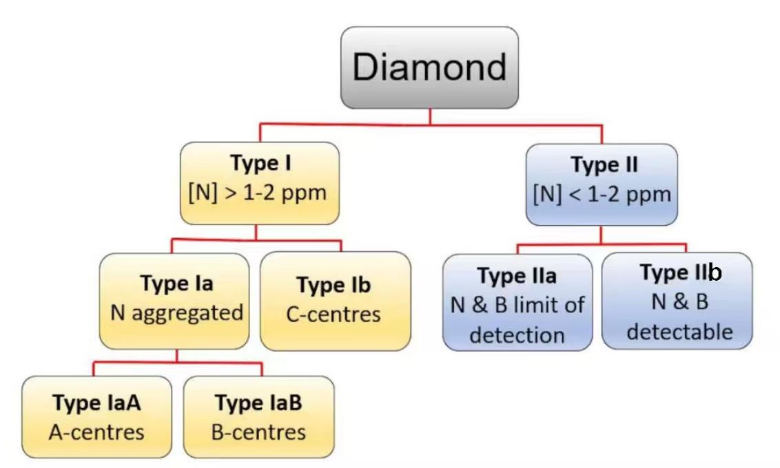
Diamonds can be classified into two major types, Type I and Type II, based on the presence and state of nitrogen impurities in their structure. Type I diamonds are characterized by a high nitrogen content, while Type II diamonds contain little to no nitrogen. Based on the form of nitrogen and other impurity differences, these two types can be further subdivided into Ia, Ib, IIa, and IIb types, as shown in Figure 1.2.
Ia-type diamonds are primarily characterized by the aggregation of nitrogen atoms and are commonly found in natural diamonds. It has two subtypes: IaA and IaB. In IaA-type diamonds, nitrogen exists in the form of A-centers (pairs of substitutional nitrogen atoms), with the main infrared absorption peak around 1282 cm−1. In IaB-type diamonds, nitrogen atoms form tetrahedral B-centers, with the infrared absorption peak around 1175 cm−1. These diamonds exhibit no absorption in the visible light spectrum and are macroscopically colorless and transparent.
Ib-type diamonds are typically synthesized artificially, with nitrogen impurities dispersed in the lattice as isolated single nitrogen atoms (isolated nitrogen). Their infrared absorption peaks are found in the 1130 cm−1 and 1344 cm−1 regions. Due to their optical absorption characteristics, these diamonds often appear yellow or yellow-green. Natural Ib-type diamonds are very rare, and they are mainly produced using high-pressure, high-temperature processes. Modern synthetic techniques can precisely control their nitrogen content (ranging from several dozen to thousands of ppm).
IIa-type diamonds have very low nitrogen content (typically less than 1 ppm) and are commonly found in chemical vapor deposition (CVD) synthesis products. These diamonds appear macroscopically colorless and transparent. Their infrared spectra show no significant absorption peaks in the 1000–1400 cm−1 and 2800 cm−1 ranges.
IIb-type diamonds are blue due to trace boron impurities and exhibit P-type semiconductor properties. These diamonds are extremely rare in nature (less than 0.1%) and must be artificially doped with boron through specialized processes to achieve functional properties.
OMeda (Shanghai Omedasemi Co.,Ltd) was founded in 2021 by 3 doctors with more than 10 years of experience in nanpfabrication. It currently has 15 employees and has rich experience in nanofabrication (coating, lithography, etching, two-photon printing, bonding) and other processes. We support nanofabrication of 4/6/8-inch wafers.