The article discusses the development and demonstration of crystalline silicon-on-sapphire (c-SOS) metasurfaces that generate complex optical trap arrays for neutral atom applications. These metasurfaces are used to convert a Gaussian laser beam into arrays of optical traps, including both bright (tweezer) traps and dark (bottle-beam) traps, which are essential for applications like quantum information processing and atom-based technologies.
The primary innovation is the use of metasurfaces, which offer scalability and reduced noise compared to active optical components like spatial light modulators (SLMs) or acousto-optic deflectors (AODs). Unlike these active components, metasurfaces can produce large arrays of traps in a compact, passive form, with CMOS-compatible manufacturing processes making them easier to integrate.
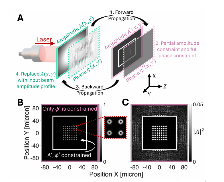
To design these metasurfaces, the Gerchberg-Saxton algorithm was adapted to optimize for both amplitude and phase profiles, enabling the generation of 3D bottle beams (dark traps) with high uniformity. The metasurfaces were fabricated and experimentally validated to generate various configurations of traps, including single-species and dual-species arrays.
Key findings include the ability to form a 7×7 dark trap array and a 21×21 bright trap array, with a further demonstration of interleaved bright and dark traps. The results suggest that these metasurfaces can be scaled to much larger arrays, with potential for integration into vacuum cells for miniaturized quantum setups.
This work positions c-SOS metasurfaces as a scalable and reliable solution for generating complex atomic trap arrays, surpassing traditional active optical methods in terms of size, power efficiency, and ease of integration into quantum devices.
OMeda (Shanghai Omedasemi Co.,Ltd) was founded in 2021 by 3 doctors with more than 10 years of experience in nanpfabrication. It currently has 15 employees and has rich experience in nanofabrication (coating, lithography, etching, two-photon printing, bonding) and other processes. We support nanofabrication of 4/6/8-inch wafers.