This article presents an integration pathway for the incorporation of barium titanate (BaTiO₃, or BTO) thin films in silicon photonics, specifically for electro-optic (EO) modulation. Barium titanate is known for its high Pockels coefficient, which is beneficial for efficient electro-optic modulation, making it an ideal material to integrate into photonic devices. The authors propose a chemical solution deposition (CSD) process to integrate these BTO thin films onto silicon photonic circuits, enabling improved performance in high-speed, low-power applications.
Key steps in the process involve:
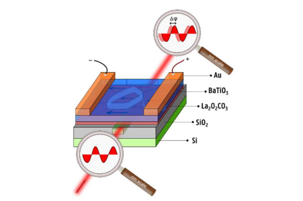
Device Fabrication: The integration begins with the fabrication of silicon waveguides on silicon-on-insulator (SOI) substrates, using electron beam lithography. Following this, hydrogen silsesquioxane (HSQ) is applied for planarization, and the BTO thin film is deposited on top using the lanthanum oxycarbonate (LOC) template film. The LOC template ensures proper growth of the BTO layer without interdiffusion into the silicon.
Device Operation and Results: The performance of the BTO thin films is characterized through both free-space and on-chip measurements. The Pockels coefficient of the BTO thin film was found to be 138.68 ± 5.78 pm/V, indicating its high electro-optic response. The BTO was successfully integrated into a silicon ring resonator, demonstrating device operation where the application of a DC voltage shifts the resonant wavelength of the ring resonator, turning it into a working electro-optic modulator.
Performance Metrics: The tuning efficiency of the modulator was measured at 2.3 pm/V, and the half-wave voltage-length product was calculated to be 9.863 V·cm. These results indicate a high performance, though further optimization of the waveguide design is suggested to reduce the high voltage-length product and improve the device's efficiency.
In conclusion, the integration of BTO thin films using CSD onto silicon photonic platforms has been successfully demonstrated, showing promising electro-optic modulation capabilities. This technique can be applied to planar and non-planar structures, offering a pathway for improving the performance and scalability of photonic integrated circuits for various high-speed, low-power applications.
OMeda (Shanghai Omedasemi Co.,Ltd) was founded in 2021 by 3 doctors with more than 10 years of experience in nanpfabrication. It currently has 15 employees and has rich experience in nanofabrication (coating, lithography, etching, two-photon printing, bonding) and other processes. We support nanofabrication of 4/6/8-inch wafers.