This article discusses a novel integration method for combining InGaAs/InP single-photon avalanche diodes (SPADs) with thin-film lithium niobate (TFLN) photonic chips using photonic wire bonding (PWB) technology. This integration approach aims to address the challenge of combining SPADs, which are essential for single-photon detection in quantum photonics, with TFLN chips, which offer excellent performance in optical modulation, low waveguide loss, and strong nonlinear effects.
Key points of the article:
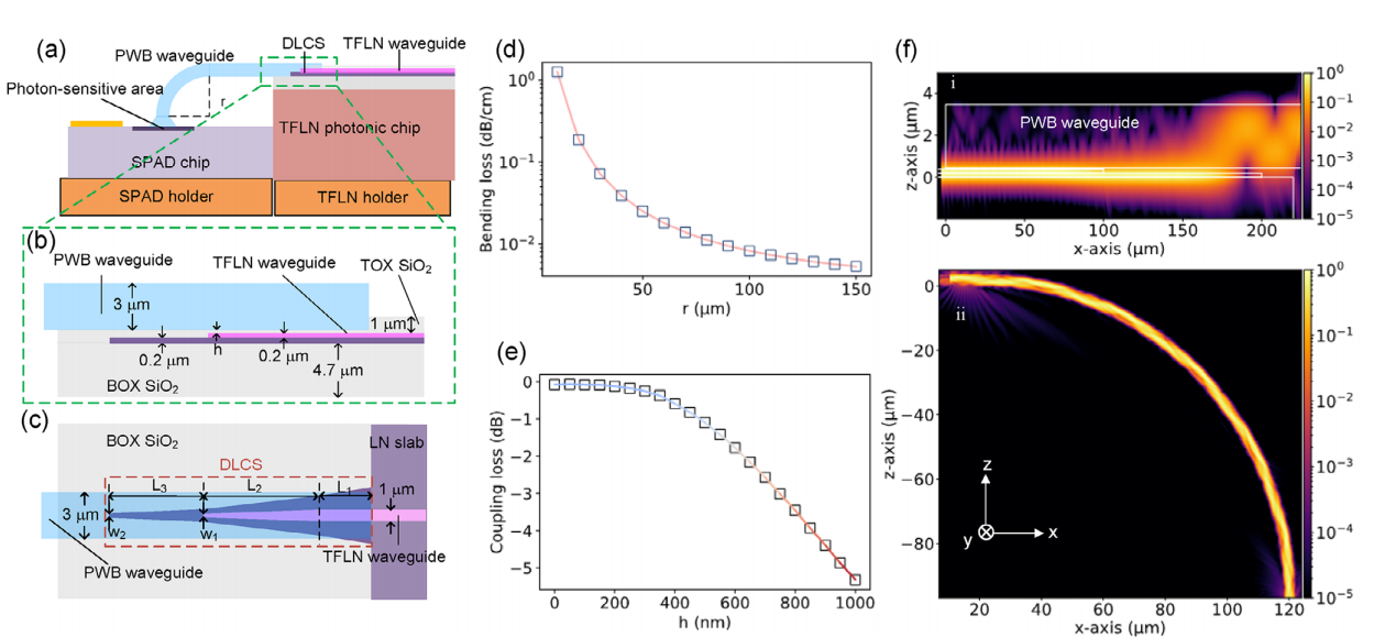
Photonic Wire Bonding (PWB) Integration: PWB is employed to create a suspended polymer waveguide, which connects the SPAD with the TFLN chip. This approach allows for flexible, low-loss, and alignment-tolerant optical coupling between the two components. The waveguide spans over 300 µm, ensuring stable connections.
Performance of the Integrated SPAD: The integrated SPAD achieves a photon detection efficiency (PDE) of 13.8% at −30°C, with low dark count rates (≈6 × 10⁻⁴ Hz/gate), a 3% after-pulse probability (APP), and a time jitter of 370 ps. These results indicate that the hybrid integration performs well for single-photon detection in quantum systems.
Advantages of PWB: The PWB technology provides significant advantages, including reduced optical alignment requirements, robustness against misalignment, and the potential for parallel integration of multiple SPADs on a single photonic chip.
Applications: This method has great potential for quantum communication systems, quantum information processing, and weak-light sensing, such as quantum key distribution (QKD) and optical time-domain reflectometry (OTDR). Additionally, it enables compact and low-cost quantum photonic systems that can be scaled for various applications.
Further Improvements: While the current integration scheme is effective, improvements in fabrication processes, such as reducing waveguide losses and optimizing the quenching circuit, could further enhance performance. Additionally, improvements in the readout circuits and the use of more advanced filters could reduce time jitter and improve detection efficiency.
In conclusion, this work presents a promising solution for the integration of SPADs and TFLN chips, advancing the development of compact and cost-effective single-photon detection systems for quantum technologies.
OMeda (Shanghai Omedasemi Co.,Ltd) was founded in 2021 by 3 doctors with more than 10 years of experience in nanpfabrication. It currently has 15 employees and has rich experience in nanofabrication (coating, lithography, etching, two-photon printing, bonding) and other processes. We support nanofabrication of 4/6/8-inch wafers.