This article explores the use of 3D printing techniques to fabricate high-quality Fresnel lenses, including both normal and holographic types, via a novel method based on masked stereolithography (MSLA). The key points from the study are:
Introduction to 3D-Printed Fresnel Lenses:
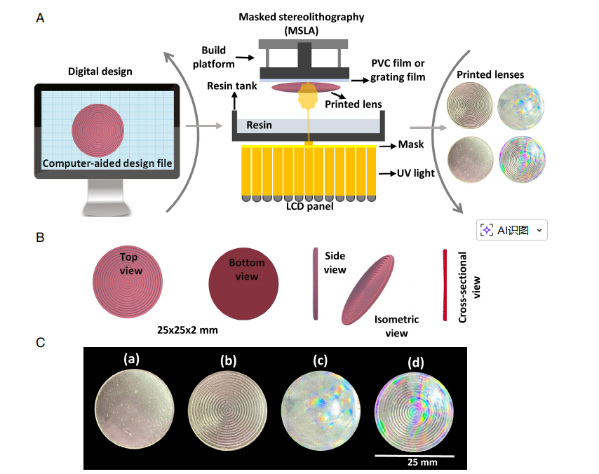
Additive manufacturing (AM), including 3D printing, is revolutionizing optical component fabrication, offering advantages such as high material efficiency and precision. Traditional methods for making Fresnel lenses involve etching or molding, but these techniques are limited by complexity and lack of flexibility in design. This paper presents a more straightforward and cost-effective method using MSLA-based 3D printing, which allows for the creation of micro/nano-structured lenses in a single step.
Fabrication Process:
The Fresnel lenses were designed using computer-aided design (CAD) software and fabricated using a 3D printer equipped with MSLA technology. This method enables the creation of fine patterns (5 μm) on the surface of the lenses, leading to their ability to focus light and produce holographic rainbow effects.
The 3D printing process was optimized using specific parameters, such as a 25-micron layer thickness and proper exposure times, to ensure the quality of the lenses. PVC film was used on the print bed to enhance surface smoothness, avoiding the need for supporting structures during printing.
Holographic Fresnel Lenses:
A key innovation in this paper is the integration of holographic microgratings directly onto the surface of the printed Fresnel lenses. This was achieved by printing the lenses on top of a holographic film, which imprints a 2D periodic grating pattern onto the lens. This results in lenses that focus light while also exhibiting a holographic diffraction effect, useful for various optical applications like miniature spectrometers.
Optical Characterization:
The transmission and diffraction properties of the 3D-printed lenses were analyzed using various optical characterization techniques, including scanning electron microscopy (SEM) and optical transmission spectroscopy. The results showed that the holographic Fresnel lenses exhibited reduced transmission compared to the normal lenses due to increased reflection and scattering from the holographic pattern.
Focal length measurements using different laser wavelengths (blue, green, and red) showed that the fabricated lenses performed well, with focal lengths within 10 mm deviation from the theoretical values. The holographic lenses also demonstrated improved focusing behavior.
Surface Quality and Hydrophobicity:
Surface roughness and the effect of surface texturing on optical performance were examined. The SEM analysis revealed that the 3D printing process achieved high-quality surface finishes with minimal defects. Surface roughness was quantified using atomic force microscopy (AFM), with values indicating that the lenses met acceptable standards for optical components.
Additionally, water absorption tests revealed that the lenses made with holographic patterns absorbed less water, likely due to the increased surface texture, which enhanced hydrophobicity.
Applications and Conclusion:
The fabricated Fresnel lenses, especially those with holographic patterns, are suitable for a wide range of optical applications, including imaging-based miniature spectrometers, optical sensing, and communications. The study demonstrates a simple, cost-effective approach to producing functional optical elements with complex geometries using 3D printing, offering significant potential for further development in optical device manufacturing.
In conclusion, this work highlights the ability to manufacture both normal and holographic Fresnel lenses using MSLA-based 3D printing technology, which could lead to advancements in optical sensing, communication, and imaging applications.
OMeda (Shanghai Omedasemi Co.,Ltd) was founded in 2021 by 3 doctors with more than 10 years of experience in nanpfabrication. It currently has 15 employees and has rich experience in nanofabrication (coating, lithography, etching, two-photon printing, bonding) and other processes. We support nanofabrication of 4/6/8-inch wafers.