Paper Download
OMedaSemi can provide diverse composite X-o-X Wafer, we use surface actived bonding technology to bond diverse material . you can click this page to know our composite wafer and our surface actived bonding technology

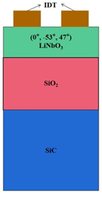
The article titled "Theoretical Optimization of Surface Acoustic Waves Resonator Based on 37°Y-47°X LiNbO₃/SiO₂/SiC Multilayered Structure" presents a study on optimizing the design of surface acoustic wave (SAW) resonators for high-frequency applications, particularly in 5G communication systems.
Objective:
The study focuses on designing a multilayer SAW resonator using a 37°Y-47°X LiNbO₃/SiO₂/SiC structure.

The goal is to achieve high electromechanical coupling coefficient (K²), high phase velocity, and near-zero temperature coefficient of frequency (TCF), which are critical for 5G applications.
Methodology:
Finite Element Method (FEM) simulations were used to optimize the thickness of LiNbO₃, SiO₂, and aluminum electrodes in the multilayer structure.
The study explores the impact of different material layer thicknesses on the resonator's performance, including K², phase velocity, and TCF.
Optimization Results:
The optimal parameters were found to be a LiNbO₃ thickness of 0.08λ, SiO₂ thickness of 0.2λ, and electrode thickness of 0.056λ.
These parameters resulted in a K² of 10.95%, a phase velocity of 5800.43 m/s, and a TCF of -0.1 ppm/°C, making it highly suitable for 5G RF filters.
Conclusions:
The optimized structure is promising for manufacturing low-loss, broadband RF SAW filters, which are essential for 5G communications.
The study suggests that the combination of LiNbO₃ with SiO₂ and SiC provides effective temperature compensation and enhanced electromechanical properties for high-frequency applications.
OMeda (Shanghai Omedasemi Co.,Ltd) was founded in 2021 by 3 doctors with more than 10 years of experience in nanpfabrication. It currently has 15 employees and has rich experience in nanofabrication (coating, lithography, etching, two-photon printing, bonding) and other processes. We support nanofabrication of 4/6/8-inch wafers.