Today we want to show 2 kind of mgo doped lnoi wafer
the spec of this two wafer is 500nm Xcut MgO LNOi -4.7umSiO2-675umSi
the left is trimmed mgo lnoi wafer and the right is mgo lnoi wafer without trimming . if you want to know about trimming ,please click this link https://en.omedasemi.com/detail/205.html
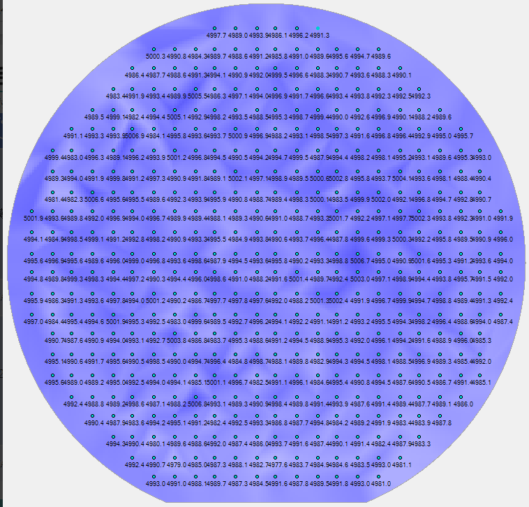
in the following picture ,we can clear see that trimming process can improve the ln layer thcikness range from 143 A to 46.3A,
more uniform surface can greatly improve production yield and also get better device performance.
Trimmed LN Layer :Avg LN Thickness:4992.4A,Range:46.3A Without Trimmed LN Layer:Avg LN Thickness:5068A,Range143A
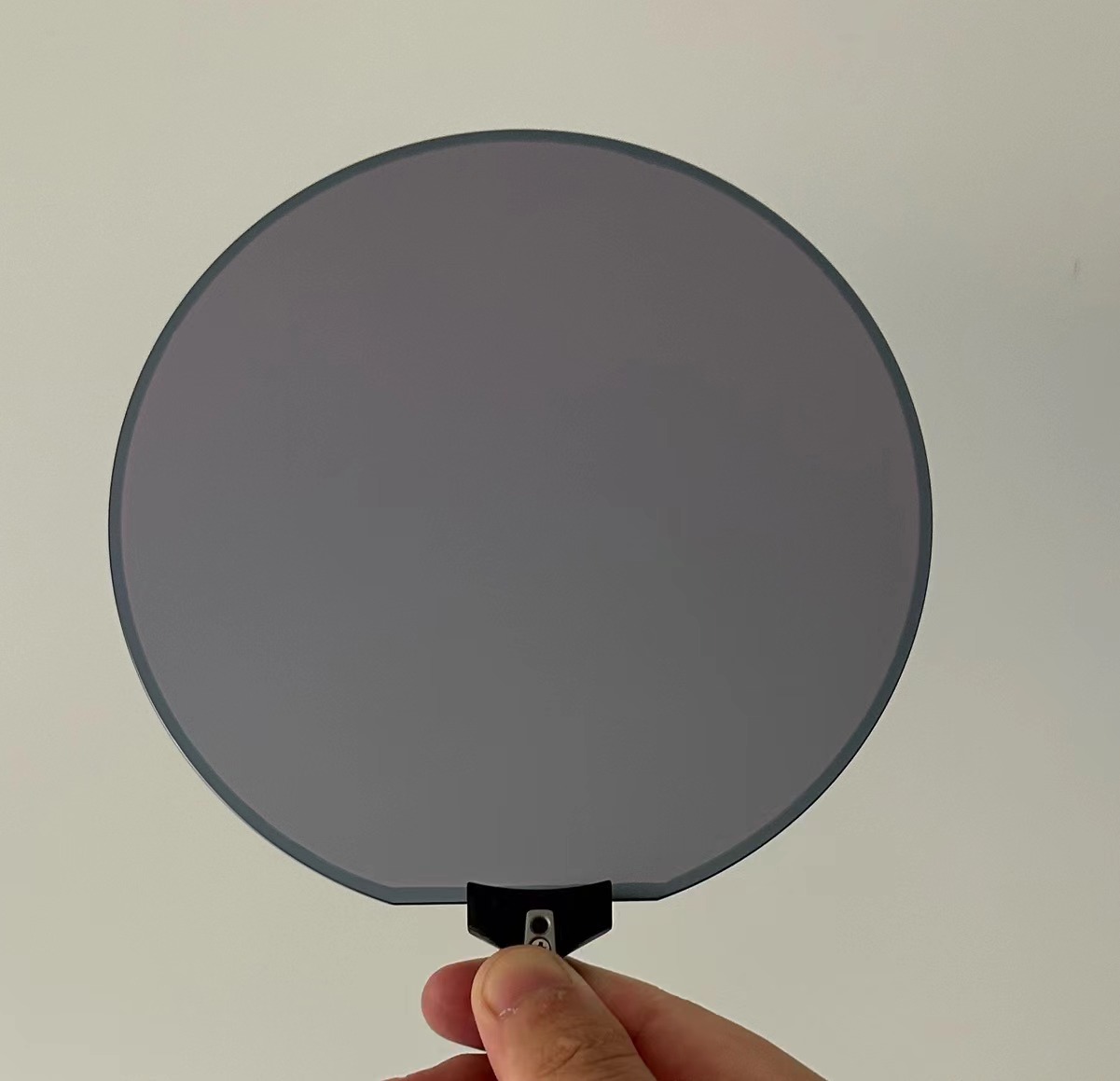
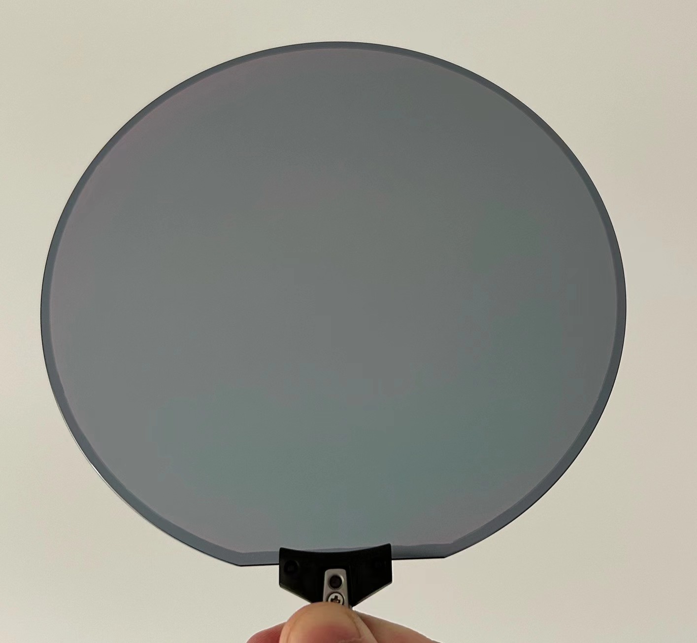
Trimmed MgO Doped LNOI Without Trimming ProcessTrimmed MgO Doped LNOI
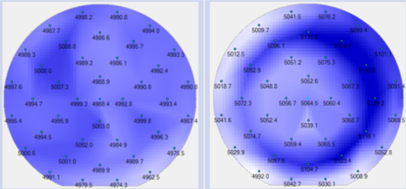
Trimmed LNOI
OMeda (Shanghai Omedasemi Co.,Ltd) was founded in 2021 by 3 doctors with more than 10 years of experience in nanpfabrication. It currently has 15 employees and has rich experience in nanofabrication (coating, lithography, etching, two-photon printing, bonding) and other processes. We support nanofabrication of 4/6/8-inch wafers.