This paper discusses advancements in GeSn (germanium tin) laser technology for use in silicon photonic chips, with a focus on the development of GeSn-on-insulator (GeSnOI) lasers. These lasers are promising candidates for addressing the need for on-chip, silicon-compatible light sources in high-speed, energy-efficient optical interconnects, particularly for data-heavy applications like artificial intelligence and high-performance computing.
Need for Efficient On-Chip Lasers:
The rapid rise in artificial intelligence and data traffic has increased the demand for fast and efficient data transmission in data centers. Co-packaged optics (CPO) is emerging as a solution, offering higher bandwidth and reduced power consumption compared to traditional electrical interconnects.
A significant challenge remains the lack of efficient, CMOS-compatible on-chip lasers, which are essential for widespread adoption of optical interconnects.
GeSn-based Lasers:
GeSn lasers have been identified as a promising solution for silicon-compatible lasers. Since their first demonstration in 2015, they have advanced significantly, overcoming the indirect bandgap limitation of traditional silicon photonics.
Recent breakthroughs in GeSn-on-insulator platforms have enabled ultra-low lasing thresholds and room-temperature operation, thanks to strain engineering and defect-free GeSn layers.
Actively Tunable GeSnOI Lasers:
Wavelength tuning capability is essential for optical communication systems using wavelength-division multiplexing (WDM). The paper discusses advancements in actively tunable GeSn lasers, which utilize mechanical strain modulation to tune the emitted wavelength.
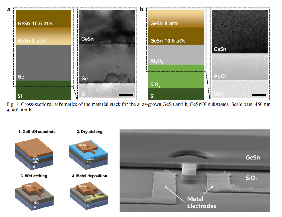
The fabrication process involves introducing a compositional gradient in the GeSn layer and bonding it to an insulator substrate (GeSnOI). This allows for precise control over the laser's emission wavelength by applying RF signals to induce periodic mechanical oscillations, which modulate the optical properties.
GeSn Nanowire Lasers:
GeSn nanowire lasers, which are based on bottom-up grown Ge/GeSn core-shell nanowires, are also presented as a promising platform for low-threshold, compact lasers. The small size of these nanowires makes them ideal for dense integration in photonic chips.
These lasers have demonstrated single-mode lasing with a low threshold (~5.3 kW/cm²) when strain engineering and cavity optimization are applied. These advancements promise efficient mid-infrared light sources for integration into silicon photonic systems.
Performance and Optimization:
The study highlights the significant improvements in the wavelength tuning range (~38 nm) and power consumption (~240 pW) for the tunable GeSn lasers, outperforming other methods like MEMS-based and thermal tuning lasers.
Optimization efforts, such as improving the nanowire cavity and enhancing strain engineering, are expected to further improve the performance of these lasers for practical on-chip deployment.
Integration with Photonic Chips:
The paper also discusses the efficient coupling of tunable GeSn laser emission into GeSn waveguides. This integration is key for the development of compact and efficient optical interconnects in future photonic chips.
The article concludes that GeSn-based lasers, especially GeSnOI lasers with active mechanical tuning and GeSn nanowire lasers, have significant potential for scalable, on-chip optical interconnects. These developments address the key challenge of integrating efficient, CMOS-compatible light sources directly onto chips, paving the way for the future of photonic integrated circuits in data centers and high-performance computing systems.
OMeda (Shanghai Omedasemi Co.,Ltd) was founded in 2021 by 3 doctors with more than 10 years of experience in nanpfabrication. It currently has 15 employees and has rich experience in nanofabrication (coating, lithography, etching, two-photon printing, bonding) and other processes. We support nanofabrication of 4/6/8-inch wafers.