This article discusses the advancements in integrated photonic circuits (PICs) and their potential to enhance connectivity for high-bandwidth applications, particularly in energy-efficient computing, data transmission, and AI systems. It focuses on the development of scalable photonic technologies aimed at overcoming the limitations of traditional electrical interconnects.
Optical Interconnect Scaling:
High-bandwidth, energy-efficient optical interconnects are crucial for AI applications that involve large data transmission across data centers.
Optical solutions, particularly co-packaged optics (CPO), have been developed to overcome the limitations of traditional electrical interconnects, offering high bandwidth, low power consumption, and improved latency.
Recent advancements have led to scalable photonic link technologies that can achieve data transfer rates in the petabit per second range. This has been made possible through multi-wavelength light sources, high-performance silicon photonics, and advanced optical-electrical packaging.
Key Technological Advancements:
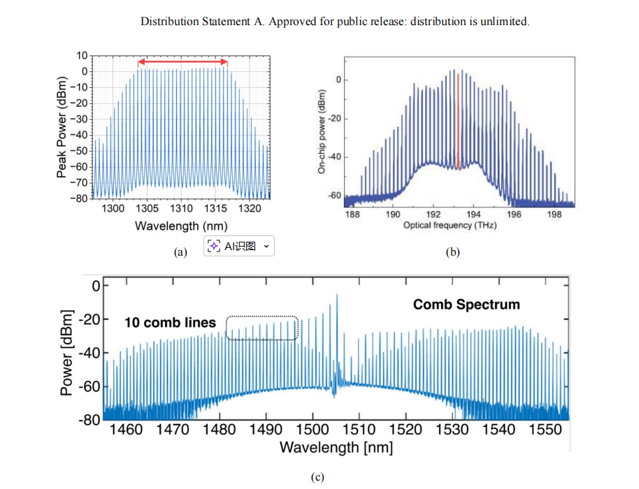
Multi-wavelength Light Sources: The development of multi-wavelength sources like Kerr microcomb technology and quantum-dot lasers enables dense wavelength-division multiplexing (DWDM), improving bandwidth by multiplexing multiple data streams onto a single fiber.
Silicon Photonics: Silicon photonic integrated circuits (PICs) have significantly increased on-chip bandwidth density. These are now small enough to be co-packaged with electronic chips, enhancing the efficiency of chip-to-chip communication.
Advanced Packaging: Innovations in multi-chip packaging have made it possible to integrate photonic chips with electronic chips, reducing the distance for electrical signals to travel and improving performance.
3D Photonic Circuits:
While current optical interconnects provide high performance, the density of photonic links within microsystems is still limited. The next step is to develop truly 3D optical routing, which would allow for more compact and efficient photonic links.
The DARPA HAPPI program is focused on enhancing link density while maintaining efficiency, predicting a three-order-of-magnitude increase in transmission density within microsystems.
3D stacking of photonic chips with multiple routing layers and advanced optical packaging will enable the integration of photonics within chips, allowing for more efficient data movement and creating new architectures for applications such as signal processing and quantum sensing.
Challenges and Innovations:
To realize this vision, new methods for optical routing, including vertical waveguides and low-loss optical vias, are needed. These innovations will help in creating compact, non-blocking optical routing systems.
Additionally, efficient chip-to-chip interconnection will require overcoming challenges such as strict alignment tolerances due to shrinking mode sizes.
Technical Approach and Ecosystem Maturation:
The HAPPI program is developing low-loss, high-density optical waveguiding and coupling solutions, targeting 1-dB link loss in large waveguide arrays. It also focuses on achieving crosstalk of <-20 dB and an optical bandwidth greater than 100 nm.
The program leverages silicon photonics platforms for telecom and data wavelengths and explores new methods for etching and direct-writing optical waveguides to improve chip-to-chip interconnects.
Applications:
The development of 3D photonic microsystems will enable advances in edge computing, AI, quantum sensing, and digital compute. The ability to route light and data efficiently within photonic chips will significantly enhance performance for future technologies.
The envisioned ecosystem for these photonic technologies includes foundries, automated design tools, packaging, and assembly capabilities, ensuring their widespread use across government and industry sectors.
This work emphasizes the importance of 3D integration and scalable photonic technologies for next-generation AI and computing applications. By enhancing optical interconnects and addressing key technical challenges such as photonic link density and chip-to-chip connectivity, these advancements will enable the creation of energy-efficient, high-bandwidth systems suitable for large-scale, data-heavy environments like data centers.
OMeda (Shanghai Omedasemi Co.,Ltd) was founded in 2021 by 3 doctors with more than 10 years of experience in nanpfabrication. It currently has 15 employees and has rich experience in nanofabrication (coating, lithography, etching, two-photon printing, bonding) and other processes. We support nanofabrication of 4/6/8-inch wafers.