Capability introduction (must read):
Size: 4 inches, 6 inches, 8 inches
Device layer tolerance: +-10nm (6inch ordinary level), +-20nm (8inch ordinary level), +-5nm (high precision with trimming process ,Know more:Trimming Process Introduction)
Top silicon layer thickness: 30nm-1500nm (SMARTCUT process) Greater than 600nm (thinning and polishing + finishing process, because the thinning and polishing process is used, the thickness can be very thick)
Thermal oxide layer thickness: 50nm-500nm (dry thermal oxide), 500nm-20um (wet thermal oxide)
Substrate thickness: customizable
Application:
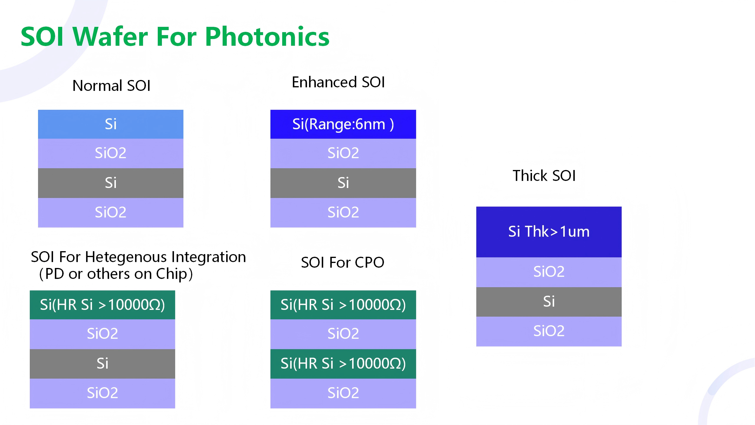
SOI Wafer For Photonics Integrated Circuit (Smartcut):
220nmSi-3umSiO2-525um/675um/725um Si (Thin film silicon photonics) --in Stock
3umSi-3umSiO2-525um/675um/725um Si (Thick film silicon photonics) --in Stock
the mostly used is 220nmSi-3umSiO2-525um/675um/725um Si (Thin film silicon photonics) and 3umSi-3umSiO2-525um/675um/725um Si (Thick film silicon photonics) and also other customized spec soi wafer .
Innovation:Also recently ,SOI wafer for photonics and Quantum with high resisitivity silicon is more and more popular ,OMedaSemi also can provide this kind SOi wafer ,the device layer and handle layer's resisitivity is bigger than 10k ohm*cm.
"Quantum devices typically require High Resistivity silicon wafers to minimize microwave losses, improving qubit coherence and the performance of control circuits."
OMeda (Shanghai Omedasemi Co.,Ltd) was founded in 2021 by 3 doctors with more than 10 years of experience in nanpfabrication. It currently has 15 employees and has rich experience in nanofabrication (coating, lithography, etching, two-photon printing, bonding) and other processes. We support nanofabrication of 4/6/8-inch wafers.