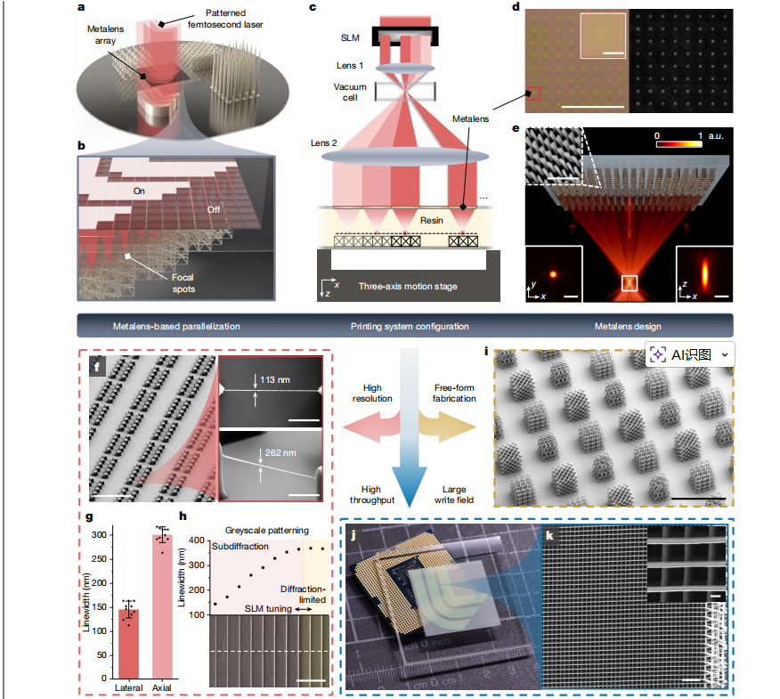
The article discusses advancements in three-dimensional (3D) nanolithography using two-photon polymerization (TPL) techniques, focusing on increasing throughput and resolution for scalable fabrication. The primary innovation is the use of a metalens array to generate multiple cooperative focal spots for parallel printing, significantly enhancing throughput beyond conventional TPL methods.
Key points:
High-throughput Parallelization: The proposed method uses a metalens array to generate over 120,000 focal spots, enabling simultaneous polymerization across a large area with a throughput of 1.2 × 10^8 voxels/s, achieving feature sizes as small as 113 nm. This approach surpasses previous limitations in both speed and precision.
Adaptive Parallel Printing: The system incorporates a spatial light modulator (SLM) to control the intensity and shape of the laser, allowing for adaptive printing strategies that optimize throughput while maintaining high precision.
Large-scale Metamaterial Fabrication: The paper demonstrates the ability to print complex mechanical and photonic metamaterials, including those with novel microarchitectures like chainmail lattices, which exhibit improved toughness and fracture resistance.
Applications and Scaling: The method is scalable, with the potential to extend to wafer-scale production for use in microelectronics, biomedicine, quantum technologies, and more. The technique enables the fabrication of a wide range of functional materials and devices at unprecedented speeds and precision.
This breakthrough in metalens-based TPL addresses key challenges in scaling 3D nanofabrication, enabling high-volume production of complex structures with applications across multiple fields.
OMeda (Shanghai Omedasemi Co.,Ltd) was founded in 2021 by 3 doctors with more than 10 years of experience in nanpfabrication. It currently has 15 employees and has rich experience in nanofabrication (coating, lithography, etching, two-photon printing, bonding) and other processes. We support nanofabrication of 4/6/8-inch wafers.