The article discusses the development and performance of broadband, monolithically integrated, waveguide-coupled photodetectors within a submicrometer-wavelength silicon photonics platform. Key findings include:
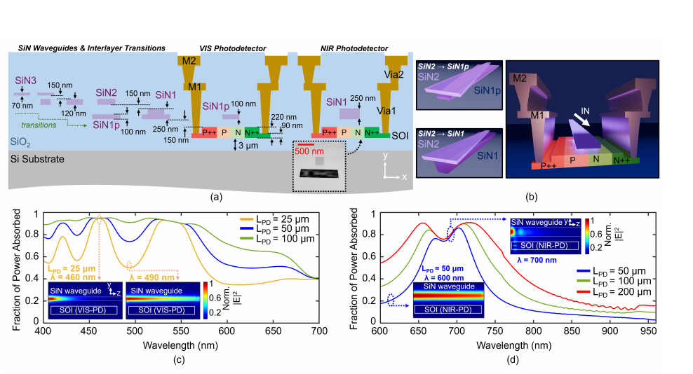
Device Structure and Operation: The photodetectors use silicon nitride (SiN) waveguides coupled over doped silicon detectors, exciting hybrid modes that enhance their absorption characteristics. Two detector variants span wavelength ranges from 400 to 748 nm and 749 to 955 nm, achieving external quantum efficiencies (EQE) of over 60% and 12%, respectively.
Performance Metrics: These devices demonstrate low dark currents (<2 pA at a 2 V reverse bias), high linear dynamic ranges (>50 dB), and optoelectronic bandwidths up to 18 GHz. Additionally, the photodetectors operate in avalanche mode with a gain-bandwidth product (GBP) as high as 374 GHz.
Applications: The devices show promise in short-wavelength systems requiring high-speed, low-noise detection, such as biophotonics (e.g., optical coherence tomography, biomolecule sensing), quantum photonics, and underwater communication.
Technical Insights: The article highlights the design considerations that improve device performance, such as optimizing the SiN waveguide thickness and geometry to match the spectral range of interest. It also notes the challenges of avalanche-mode operation, including drift in current-voltage characteristics near breakdown, suggesting that future work will focus on improving stability and enhancing avalanche-mode bandwidth.
In conclusion, this research provides a significant step toward scalable photonic integrated circuits (PICs) that can operate at short wavelengths, with potential for use in a variety of high-performance optical systems. Further optimization is anticipated to improve efficiency, speed, and stability for applications across visible and near-infrared light spectrums.
OMeda (Shanghai Omedasemi Co.,Ltd) was founded in 2021 by 3 doctors with more than 10 years of experience in nanpfabrication. It currently has 15 employees and has rich experience in nanofabrication (coating, lithography, etching, two-photon printing, bonding) and other processes. We support nanofabrication of 4/6/8-inch wafers.