The article discusses the development and characterization of Piezoelectric Micromachined Ultrasonic Transducers (PMUTs) fabricated using Enhanced Cavity Silicon-On-Insulator (EC-SOI) wafers. These PMUTs are designed to operate at 7 MHz in water and 9.5 MHz in air and are intended for various applications such as medical imaging and flow measurement.
PMUT Design and Fabrication:
A PMUT array with a size of 2.05 x 2.05 mm² was developed using an AlN-based piezoelectric layer.
The design aimed for uniform performance across the array, with each cell having a membrane diameter of 70 µm and a device layer thickness of 2.5 µm.
The fabrication process involved sputtering molybdenum (Mo) for the bottom electrode, AlN for the piezoelectric layer, and AlSi for the top electrode.
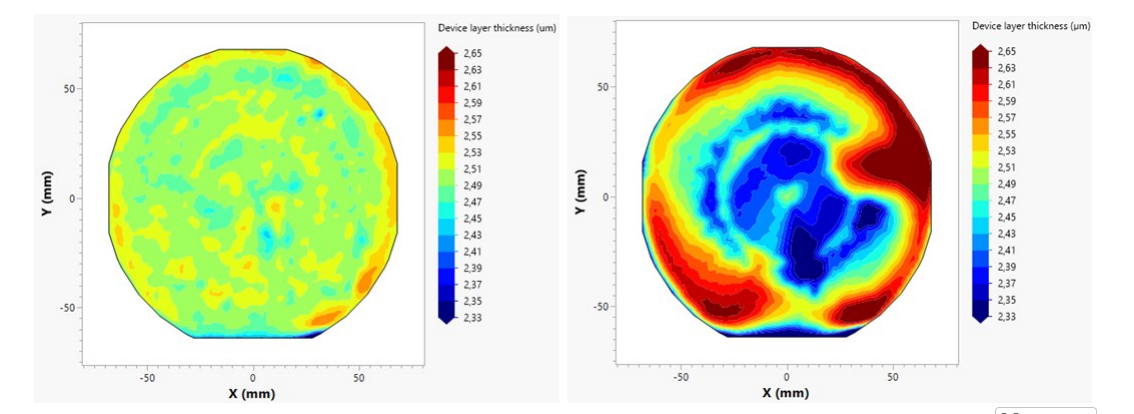
Enhanced C-SOI Wafer:
EC-SOI wafers were developed by adding extra steps to the C-SOI process to improve uniformity in the device layer thickness, achieving a uniformity of 2.5 ± 0.1 µm compared to the standard C-SOI wafers at 2.5 ± 0.3 µm.
The process steps for EC-SOI wafers included local removal of material from the device layer, enhancing the consistency of PMUT performance across the wafer.
Characterization:
Wafer-level impedance measurements showed that 41 out of 44 PMUTs fabricated on EC-SOI wafers were functional, indicating a yield of over 90%.
The resonance frequency variation for PMUTs on EC-SOI wafers was less than 3.5%, with more than 95% of the chips showing less than 2% variation, a significant improvement over PMUTs fabricated on standard C-SOI wafers (which showed up to 12% variation).
Acoustic characterization of the PMUT array demonstrated a transmit sensitivity of 6.9 kPa/V and a bandwidth of 2.8 MHz at 7.4 MHz resonance frequency in water.
Acoustic Testing:
The acoustic testing setup used Onda’s AIMS III acoustic scanning tank to measure the pressure generated by the PMUT array, with a hydrophone measuring 24 kPa at a distance of 8 mm at resonance.
The study highlights the significant advantages of EC-SOI wafers in improving frequency uniformity and overall performance of PMUT devices, making them suitable for high-performance applications. The uniformity in device layer thickness achieved through EC-SOI fabrication led to enhanced resonance frequency stability and a higher yield, demonstrating the promising potential for EC-SOI wafers in the development of PMUTs for applications in medical imaging, flow measurement, and other ultrasonic sensing technologies.
OMeda (Shanghai Omedasemi Co.,Ltd) was founded in 2021 by 3 doctors with more than 10 years of experience in nanpfabrication. It currently has 15 employees and has rich experience in nanofabrication (coating, lithography, etching, two-photon printing, bonding) and other processes. We support nanofabrication of 4/6/8-inch wafers.